Germanium photodetector and method of fabricating the same

a germanium photodetector and micro-structure technology, applied in the field of photodetectors, can solve the problems of degrading the performance of the detector, difficult to grow a low-defect germanium epitaxial layer directly on a silicon substrate, and many inherent crystal defects

Active Publication Date: 2010-04-29
ELECTRONICS & TELECOMM RES INST
View PDF12 Cites 26 Cited by
  • Summary
  • Abstract
  • Description
  • Claims
  • Application Information

AI Technical Summary

Problems solved by technology

Therefore, it is difficult to grow a low-defect germanium epitaxial layer directly on a silicon substrate.
However, the buffer layer has many inherent crystal defects, and the buffer layer must be thick enough to grow the germanium epitaxial layer.
Therefore, the buffer layer degrades the detector's performance and also imposes many restrictions on the fabrication process.
Thus, due to the high-temperature annealing process, the method is low in productivity and has a limitation in mass production.

Method used


Image

  • Germanium photodetector and method of fabricating the same
  • Germanium photodetector and method of fabricating the same
  • Germanium photodetector and method of fabricating the same

Examples


Embodiment Construction

[0016]Preferred embodiments of the present invention will be described below in more detail with reference to the accompanying drawings. The present invention may, however, be embodied in different forms and should not be constructed as limited to the embodiments set forth herein. Rather, these embodiments are provided so that this disclosure will be thorough and complete, and will fully convey the scope of the present invention to those skilled in the art.

[0017]It will be understood that when a layer (or film) is referred to as being ‘on’ another layer or substrate, it can be directly on the other layer or substrate, or intervening layers may also be present. Also, though terms like a first, a second, and a third are used to describe various regions and layers in various embodiments of the present invention, the regions and the layers are not limited to these terms. These terms are used only to tell one region or layer from another region or layer.

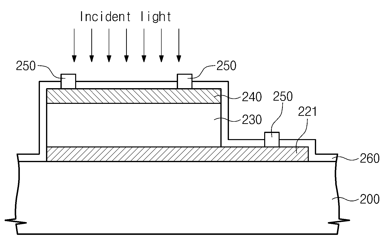
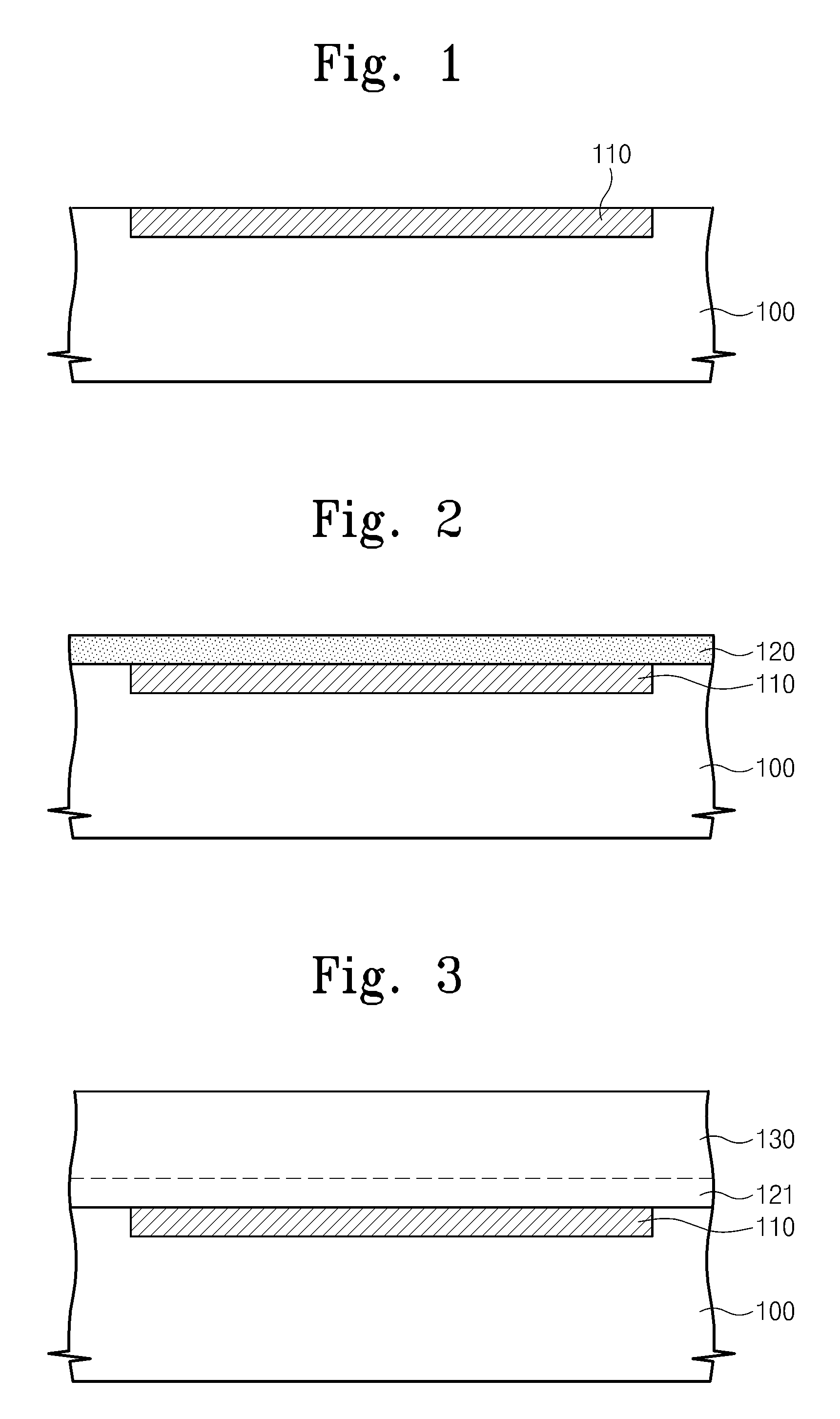
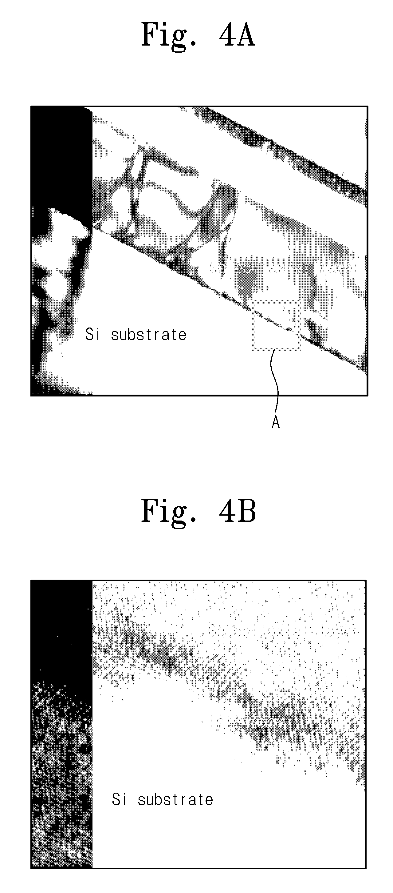
[0018]FIGS. 1 to 3 and 6 to 8 are ...


PUM

PropertyMeasurementUnit
temperatureaaaaaaaaaa
thicknessaaaaaaaaaa

Abstract

Provided is a germanium photodetector having a germanium epitaxial layer formed without using a buffer layer and a method of fabricating the same. In the method, an amorphous germanium layer is formed on a substrate. The amorphous germanium layer is heated up to a high temperature to form a crystallized germanium layer. A germanium epitaxial layer is formed on the crystallized germanium layer.

Description

CROSS-REFERENCE TO RELATED APPLICATIONS[0001]This U.S. non-provisional patent application claims priority under 35 U.S.C. §119 of Korean Patent Application No. 10-2008-0105199, filed on Oct. 27, 2008, the entire contents of which are hereby incorporated by reference.BACKGROUND OF THE INVENTION[0002]The present invention disclosed herein relates to a photodetector and a method of fabricating the same, and more particularly, to a germanium photodetector and a method of fabricating the same.[0003]Recent silicon-based optical communication technology uses germanium in both of the active device and passive device applications. Because the band gap energy (0.67 eV) of the germanium is smaller than the band gap energy (1.12 eV) of the silicon, the germanium can detect generic optical communication wavelengths λ of 1.3 μm to 1.6 μm that cannot be detected by the silicon. However, the germanium has a lattice constant difference of 4% from the silicon. Therefore, it is difficult to grow a low...

Claims


Application Information

Patent Timeline
Patent Type & Authority Applications(United States)
IPC IPC(8): H01L33/00H01L21/20
CPCH01L21/02381H01L21/0245H01L21/02532H01L21/02592H01L21/0262H01L31/028H01L31/103H01L31/1808H01L31/1872Y02E10/50H01L21/02667Y02P70/50H01L27/04H01L27/14H01L31/18
Inventor SUH, DONGWOOKIM, SAM HOONKIM, GYUNGOCKJOO, JIHO
Owner ELECTRONICS & TELECOMM RES INST
Why Eureka
Try Eureka