
Semiconductor device manufacturing method, semiconductor device and semiconductor device manufacturing installation

Inactive Publication Date: 2010-04-29
APPLIED MATERIALS INC
View PDF2 Cites 27 Cited by
  • Summary
  • Abstract
  • Description
  • Claims
  • Application Information

AI Technical Summary

Benefits of technology

[0010]According to a further embodiment, a semiconductor device manufacturing installation is provided, including a coating device adapted for coating a semiconductor substrate, a heating device adapted for annealing the coated semiconductor substrate, and a control device adapted for controlling the coating device and the heating device and adapte

Problems solved by technology

This results in undesirable recombination of charge carriers,

Method used


Image

  • Semiconductor device manufacturing method, semiconductor device and semiconductor device manufacturing installation
  • Semiconductor device manufacturing method, semiconductor device and semiconductor device manufacturing installation
  • Semiconductor device manufacturing method, semiconductor device and semiconductor device manufacturing installation

Examples


Example

DETAILED DESCRIPTION OF THE DRAWINGS

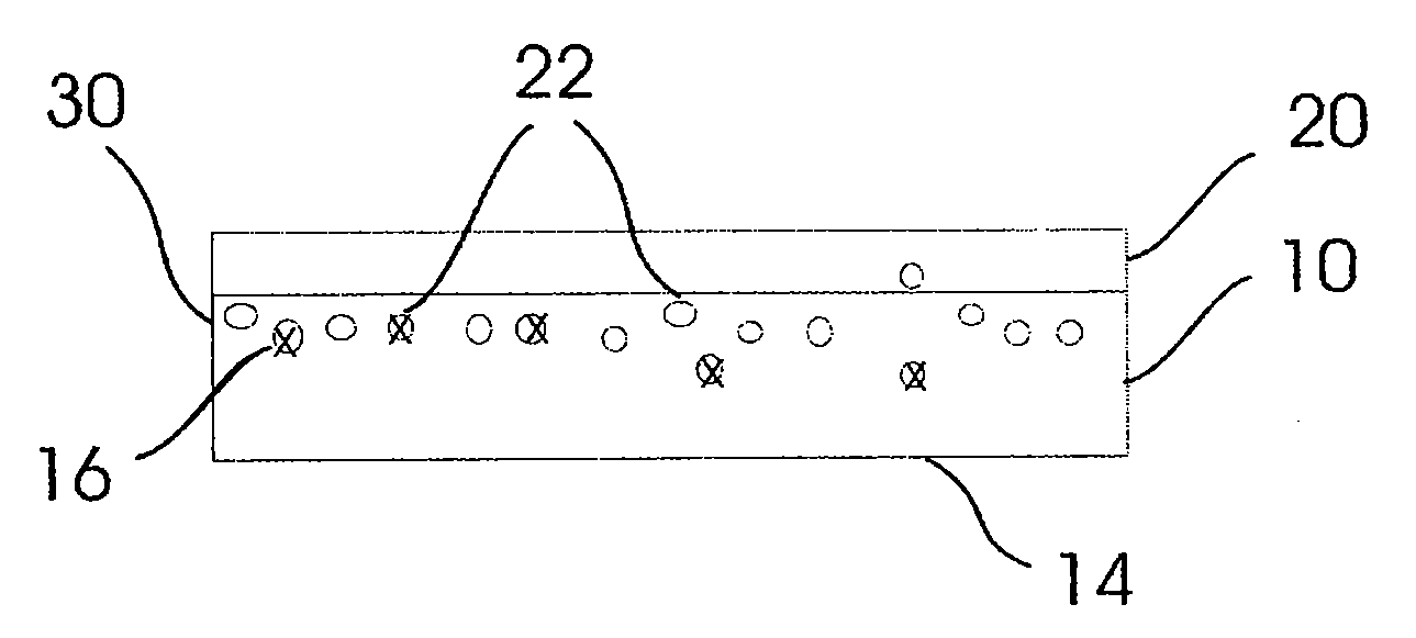
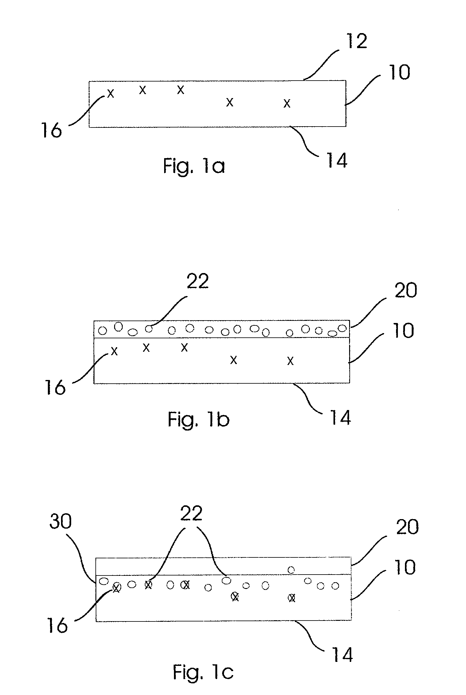
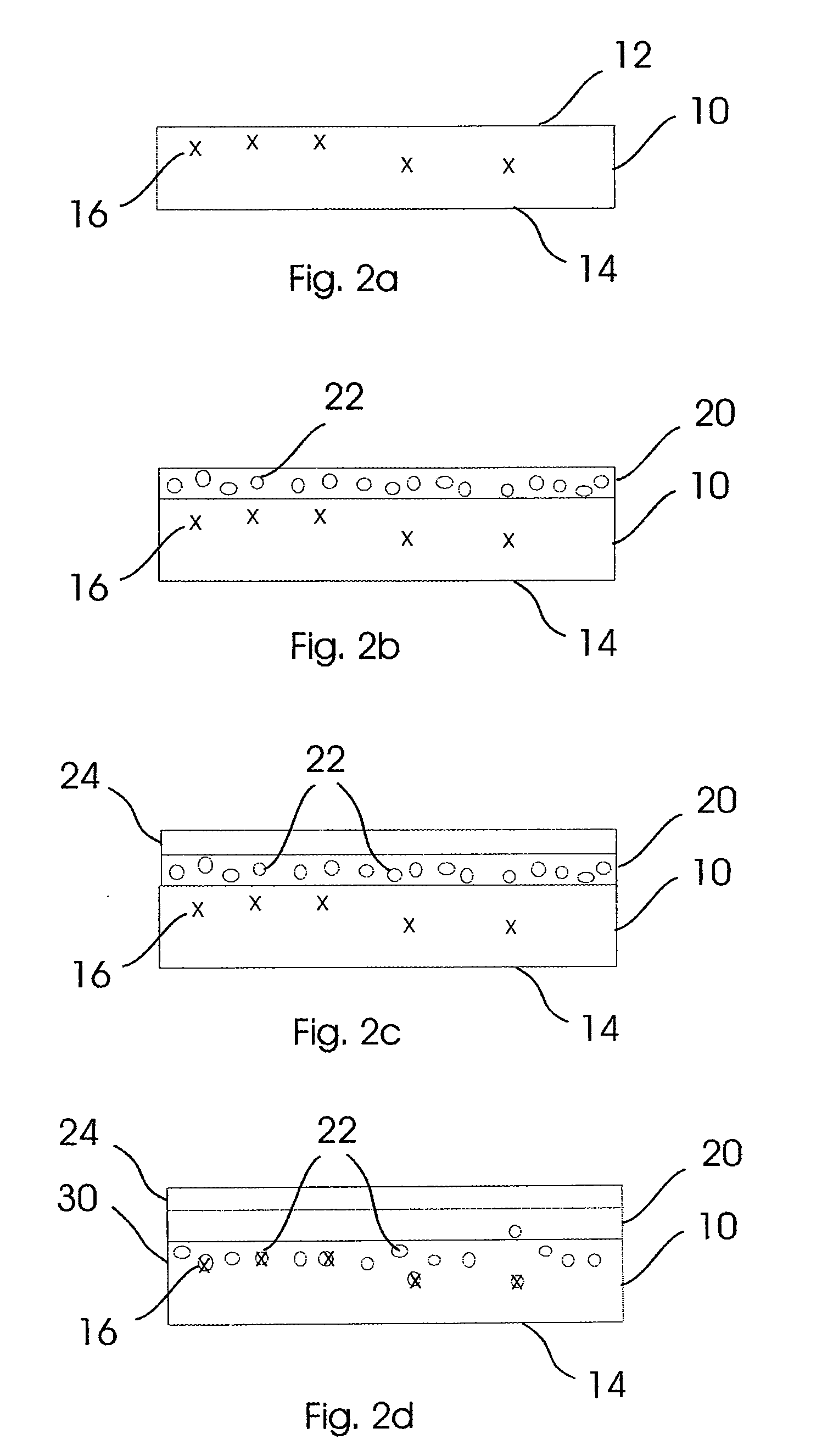
[0018]Reference will now be made in detail to the various embodiments, one ore more examples of which are illustrated in the figures. Each example is provided by way of explanation, and is not meant as a limitation of the invention.

[0019]Without limiting the scope, in the following, the semiconductor device will exemplarily be referred to as solar cell. Moreover, without limiting the scope, the substrate of the semiconductor device will exemplarily be referred to as wafer or silicon wafer, also referred to as a silicon substrate. However, examples of embodiments disclosed herein may also be applied to other types of semiconductor devices, such as thin-film solar cells. Moreover, other semiconductors or semiconductor materials than silicon may be contemplated. Further, without limiting the scope, in the following, the silicon wafer will exemplarily be referred to as a multi-crystalline p-type silicon wafer. However, other types of silicon wafers ma...


PUM


Abstract

A semiconductor device manufacturing method is provided, including: providing a semiconductor substrate, forming on the semiconductor substrate a layer including a semiconductor compound and a dope additive, and thereafter forming an emitter region and gettering impurities by annealing the semiconductor substrate including the layer.

Description

FIELD OF THE INVENTION[0001]Embodiments of the invention relate to semiconductor devices, for instance to solar cells. They relate particularly to a semiconductor device manufacturing method, a semiconductor device and a semiconductor device manufacturing installation.BACKGROUND OF THE INVENTION[0002]Semiconductor devices have many functions in a plurality of industrial fields, including, but not limited to, fabrication of electronic devices, such as transistors, and photovoltaic cells, such as solar cells. Individual photovoltaic cells are e.g. used for powering small devices such as electronic calculators. Photovoltaic arrays are used for instance in remote area power systems, earth-orbiting satellites and space probes, remote radiotelephones and water pumping applications.[0003]The principle of operation of a solar cell containing a p-n junction can be roughly described as follows. The solar cell absorbs light and generates electron / hole charge pairs due to absorbed light energy....

Claims


Application Information

Patent Timeline
IPC IPC(8): H01L21/322
CPCH01L21/3221H01L31/068H01L31/186Y02E10/547H01L31/1804Y02P70/50
Inventor FERRE I TOMAS, RAFEL
Owner APPLIED MATERIALS INC
Features
  • Generate Ideas
  • Intellectual Property
  • Life Sciences
  • Materials
  • Tech Scout
  • Unparalleled Data Quality
  • Higher Quality Content
  • 60% Fewer Hallucinations
Learn More