

Semiconductor memory device
a memory device and semiconductor technology, applied in the field of semiconductor memory devices, can solve the problems of data deterioration resulting from read disturbance, physical deterioration of gate dielectric films, electric charge,
- Summary
- Abstract
- Description
- Claims
- Application Information
AI Technical Summary
Benefits of technology
Problems solved by technology
Method used
Image

Examples
first embodiment
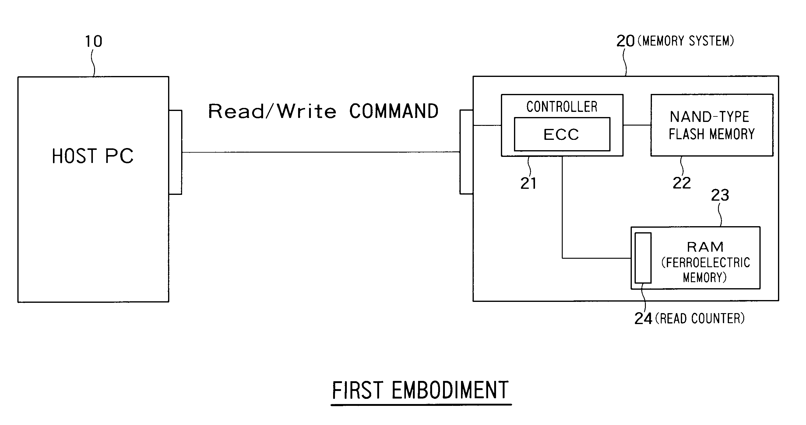
[0026]FIG. 1 is a block diagram showing a configuration of a memory system 20 according to a first embodiment of the present invention. The memory system 20 is communicably connected to a host PC 10. In response to a read command or a write command from the host PC 10, the memory system 20 performs a data read operation or a data write operation according to the command.
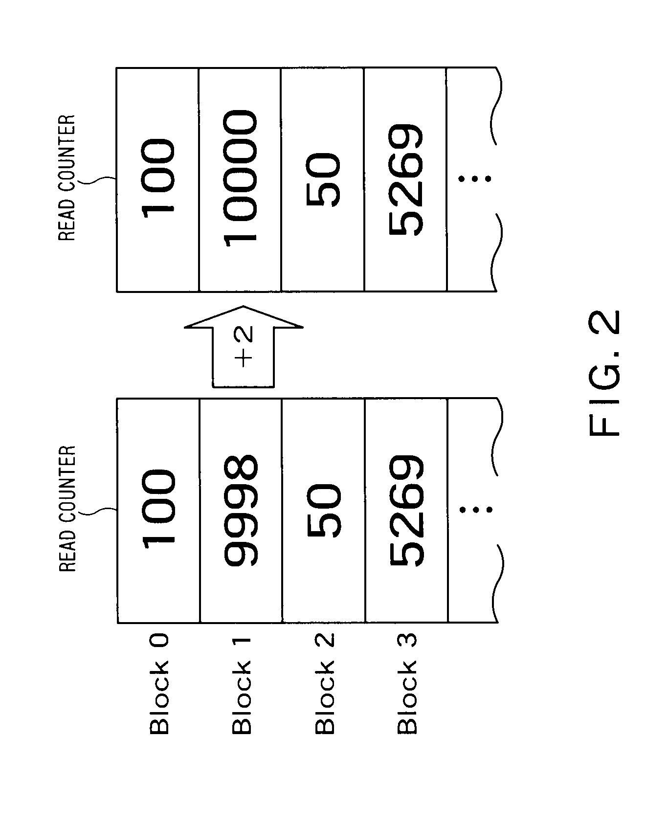
[0027]The memory system 20 includes a controller 21 serving as a control unit, a NAND flash memory (hereinafter, “NAND memory) 22 serving as a first memory device, and a ferroelectric memory (hereinafter, “RAM”) 23 serving as a second memory device.
[0028]The NAND memory 22 is, for example, an EEPROM type nonvolatile memory and used as a main storage memory. The NAND memory 22 is configured to include blocks each including a plurality of pages, and each page includes a plurality of bits stored in a plurality of memory cells (i.e., includes a plurality of memory cells). A data write operation or a data read operation i...
second embodiment
[0043]FIG. 5 is a block diagram showing a configuration of a memory system 20 according to a second embodiment of the present invention. The second embodiment differs from the first embodiment in that the RAM 23 includes a write counter 25 and a second threshold register 26. Other configurations according to the second embodiment can be the same as those according to the first embodiment.
[0044]FIG. 6 is a conceptual diagram showing configurations of the read counter 24, the write counter 25, and the second threshold register 26. The write counter 25 stores therein the number of erases (the number of writes) for a write target block for every block. Namely, since data is erased from a certain block before data is written to the certain block in the NAND flash memory 22, the write counter 25 calculates an erase count (a write count) for this certain block. The write counter 25 is included in the nonvolatile RAM 23, so that loss of information on the erase counts (the write counts) doe...
third embodiment
[0052]FIG. 8 is a block diagram showing a configuration of a memory system 20 according to a third embodiment of the present invention. FIG. 9 is a conceptual view showing a read counter 24 and a second threshold register 26. FIG. 10 is a flowchart showing an operation performed by the memory system 20. In the third embodiment, the second threshold is changed according to an error bit count detected by an ECC circuit and a data error direction. The third embodiment, therefore, differs from the second embodiment by including the second threshold register 26. Other configurations according to the third embodiment can be the same as those according to the first embodiment.
[0053]The data error direction indicates either an instance (an error direction 1) where a logic value changes from 0 to 1 or an instance (an error direction 2) where a logic value changes from 1 to 0. It is defined, for example, that a state where many electrons are accumulated in a floating gate of a memory cell is ...
PUM
 Abstract
Description
Claims
Application Information