Electronic device and lid

a technology of electronic devices and lids, applied in semiconductor devices, semiconductor/solid-state device details, electrical apparatus, etc., can solve the problems of lid , lid , adhesive , etc., and achieve the effect of preventing the lid from

Active Publication Date: 2010-05-06
RENESAS ELECTRONICS CORP
View PDF11 Cites 34 Cited by
  • Summary
  • Abstract
  • Description
  • Claims
  • Application Information

AI Technical Summary

Benefits of technology

[0014]In this way, the lid can be adhered to the substrate without being tilted against the substrate by arranging the protrusion portion on part of the flange portion of the lid to press the lid against the substrate, the protrusion portion of the lid serving as a supporting point when the lid is attached to the substrate. The interval between the substrate and the area of the flange portion other than the protrusion portion can be maintained.
[0015]As a result, the adhesive can be uniformly spread between the substrate and the area of the flange portion other than the protrusion portion, and the connection reliability of the lid can be secured. The distances between the upper sides of the electronic components and the cover portion of the lid differ depending on the heights of the electronic components. The configuration described above can improve the degree of certainty that the upper sides of the electronic components and the planar surface of the cover portion of the lid are parallel. Therefore, the distances between the upper sides of the electronic components and the planar surface of the cover portion of the lid can be accurately predicted even if electronic components with different heights are mounted on the substrate. Thus, the film thickness of the heat dissipation paste can be easily controlled to reduce the variations in the upper side heights of the heat dissipation paste, and the heat dissipation paste and the lid can sufficiently make contact. As a result, excellent heat dissipation characteristics can be provided.
[0017]The present invention can prevent the lid from tilting when the lid is attached to a substrate.

Problems solved by technology

However, conventionally, there id a problem that the lid tilts when the lid is attached to the substrate.
However, since the lid 50 contacts the heat dissipation paste 12 upon the attachment to the substrate 2, there is a problem that the lid 50 is affected by the variation in the upper side height of the heat dissipation paste 12 on the electronic components, and the lid 50 tilts upon the attachment.
However, if the lid 50 tilts and the interval between the lid 50 and the substrate 2 becomes wide, the adhesive 8 does not sufficiently spread between the substrate 2 and the lid 50, and an adhesion failure occurs.
Furthermore, when the lid 50 tilts, there may be a problem that the adhesion between the heat dissipation paste 12 and the lid 50 is insufficient, causing the heat dissipation characteristics to degrade.
Furthermore, when the lid 50 is tilted, there is a problem that the flatness defined in product specifications is not satisfied.

Method used


Image

  • Electronic device and lid
  • Electronic device and lid
  • Electronic device and lid

Examples


first embodiment

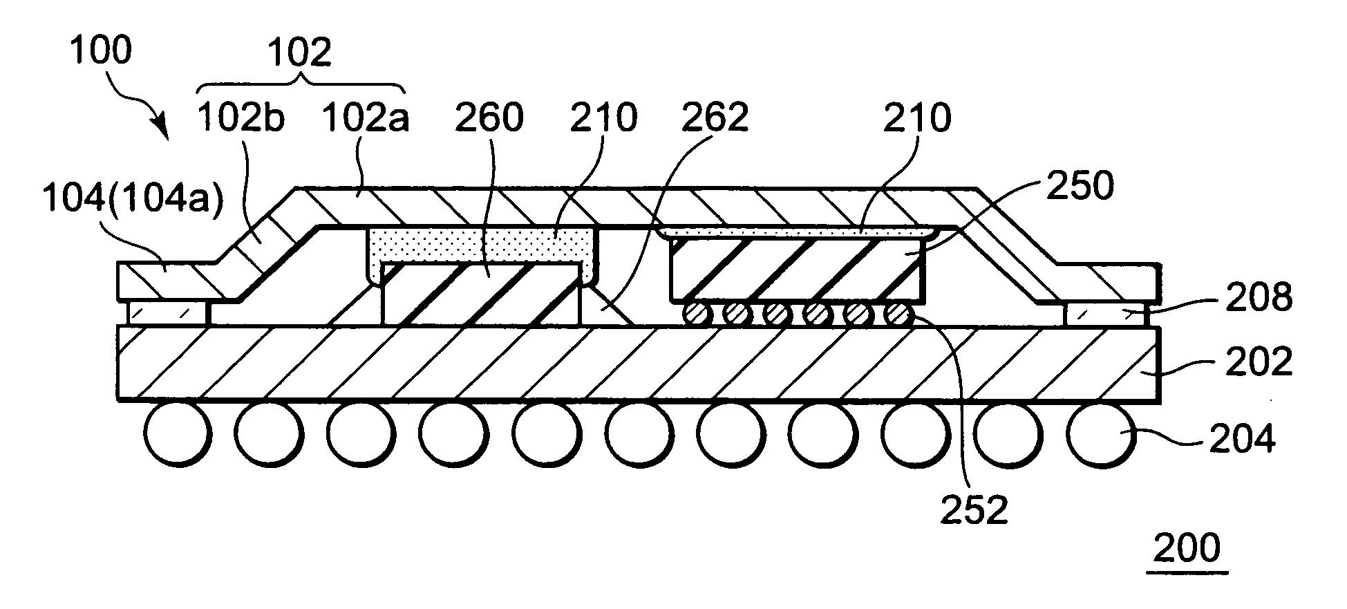
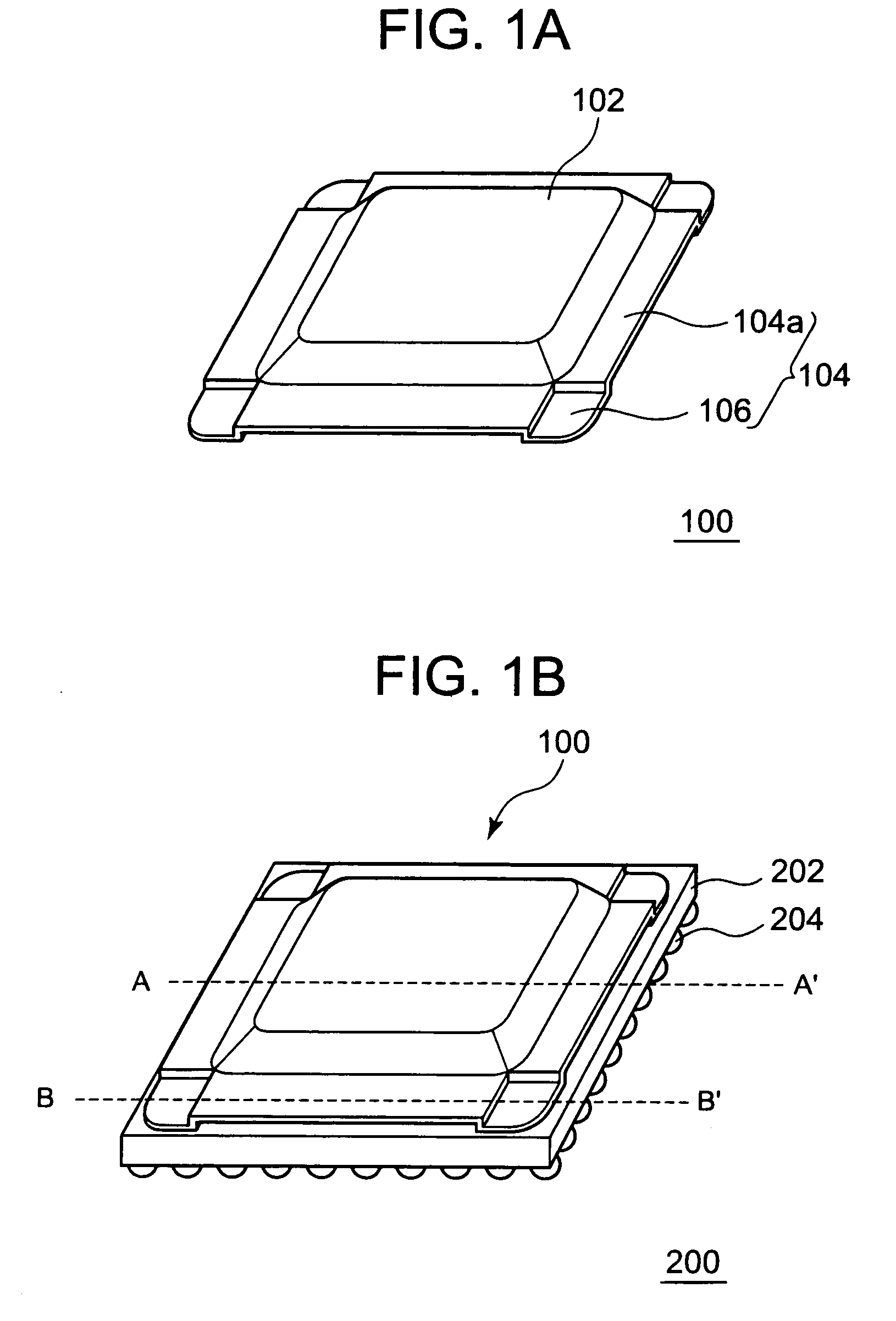
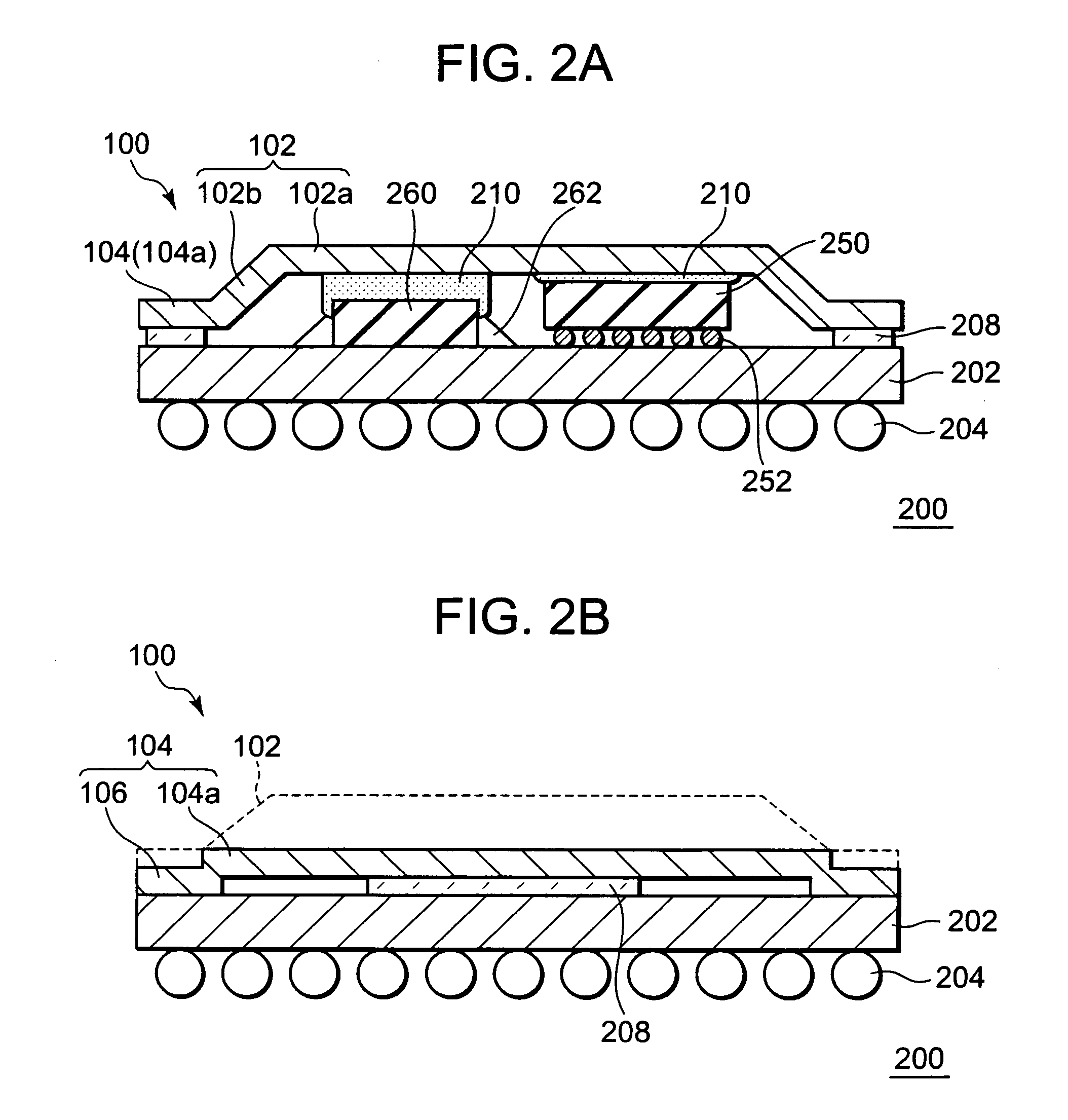
[0025]FIGS. 1A and 1B are perspective views showing a configuration of a lid 100 according to the present embodiment. FIG. 1B shows a configuration of an electronic device 200 in which a lid 100 is attached to a substrate 202. FIGS. 2A and 2B are cross sectional views showing a configuration of the electronic device 200. FIG. 2A is an A-A′ cross sectional view of FIG. 1B. FIG. 2B is a B-B′ cross sectional view of FIG. 1B.

[0026]As shown in FIG. 1A, the lid 100 includes: a cover portion 102 protruding in a first direction (upward in FIG. 1A) to cover an electronic component when the lid 100 is arranged on a substrate of an electronic device; and a flange portion 104 arranged at the periphery of the cover portion 102. The flange portion 104 includes a protrusion portion 106 protruding for a predetermined height compared to other areas in a second direction (downward in FIG. 1A) opposite the first direction. In the present embodiment, the lid 100 is adhered to the substrate through an a...

second embodiment

[0046]FIG. 6 is a perspective view showing a manufacturing procedure of an electronic device 400 in the present embodiment. In the present embodiment, the electronic device 400 includes the substrate 202, the electronic components (the first electronic component 250 and the second electronic component 260) mounted on the substrate 202, and a lid 300. The lid 300 includes a cover portion 302 protruding in a direction opposite the substrate 202 and covering the electronic components and a flange portion 304 arranged at the periphery of the cover portion 302. The cover portion 302 of the lid 300 is connected to the ground terminals 212 of the substrate 202 through the conductive resin 214.

[0047]A manufacturing procedure of the electronic device 400 will now be described.

[0048]FIG. 6A shows a configuration that the first electronic component 250 and the second electronic component 260 are mounted on the substrate 202. In the present embodiment, the ground terminals 212 are arranged at f...


PUM


Abstract

The present invention can prevent a lid from tilting when the lid is attached to a substrate. An electronic device 200 includes: a substrate 202; an electronic component mounted on the substrate 202; and a lid 100 including a cover portion 102 protruding in a direction opposite the substrate 202 and covering the electronic component and a flange portion 104 arranged at the periphery of the cover portion 102 and adhered to the substrate 202. A protrusion portion 106 protruding for a predetermined height in a direction of the substrate 202 compared to other areas of the flange portion 104 is arranged on the flange portion 104 of the lid 100.

Description

BACKGROUND OF THE INVENTION[0001]1. Field of the Invention[0002]The present invention relates to an electronic device and a lid.[0003]2. Description of the Related Art[0004]A technique for mounting electronic components such as semiconductor chips on a substrate and arranging a lid on the substrate to cover the electronic components for sealing is known.[0005]Japanese Patent Laid-Open No. 2007-42719 describes a semiconductor device comprising: a semiconductor package substrate mounted with a semiconductor element; and a lid including a concave portion and a flange portion, the concave portion accommodating the semiconductor element at a center part and including an adhesive side adhered to the semiconductor element, the flange portion located at the periphery of the concave portion and including an adhesive side adhered to the semiconductor package substrate, wherein the semiconductor package substrate and the lid cover the semiconductor element. The relationship between a depth d1 ...

Claims


Application Information

Patent Timeline
Patent Type & Authority Applications(United States)
IPC IPC(8): H01L23/04
CPCH01L23/055H01L23/10H01L23/42H01L25/0655H01L25/18H01L2224/16225H01L2924/1433H01L2924/00011H01L2924/00014H01L2224/0401
Inventor KARIYAZAKI, SHUUICHI
Owner RENESAS ELECTRONICS CORP
Why Eureka
Try Eureka