Liquid crystal display device

Inactive Publication Date: 2010-05-06
PANASONIC LIQUID CRYSTAL DISPLAY CO LTD +1
View PDF4 Cites 37 Cited by
  • Summary
  • Abstract
  • Description
  • Claims
  • Application Information

AI Technical Summary

Benefits of technology

[0020]According to the present invention, in the small-sized liquid crystal display device including the backlight in which the light emitting diode is arranged to face the edge portion of the light guide plate, it is possible to bring the light emitting diode and the edge portion of the light guide plate into close contact with each other. Due to such constitution, it is possible to increase the utilization efficiency of l

Problems solved by technology

However, there exists a limit in efforts for reducing a thickness of the liquid crystal display device by merely reducing a thickness of a glass substrate of the liquid crystal display panel or by merely

Method used


Image

  • Liquid crystal display device
  • Liquid crystal display device
  • Liquid crystal display device

Examples


embodiment 1

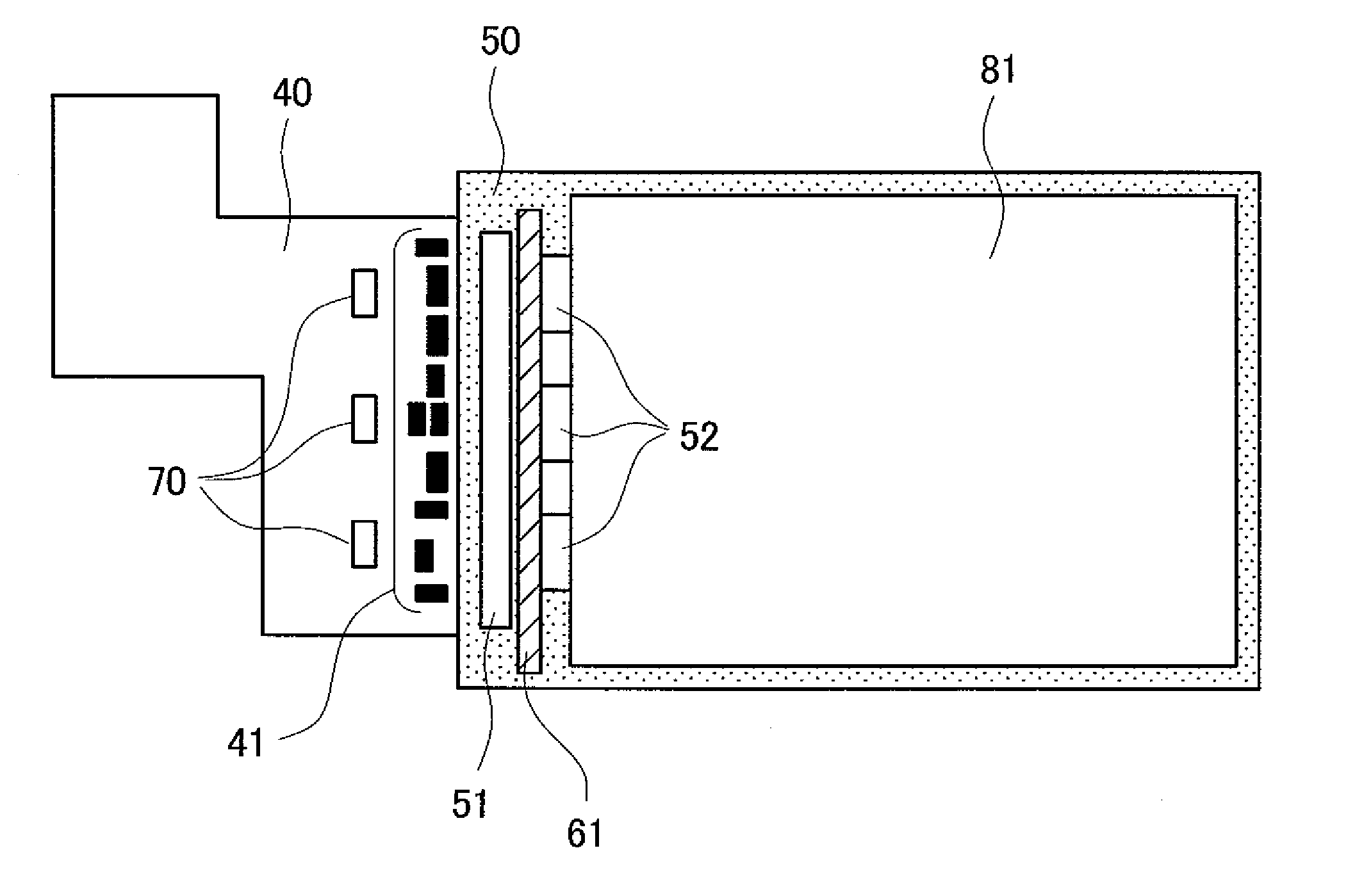
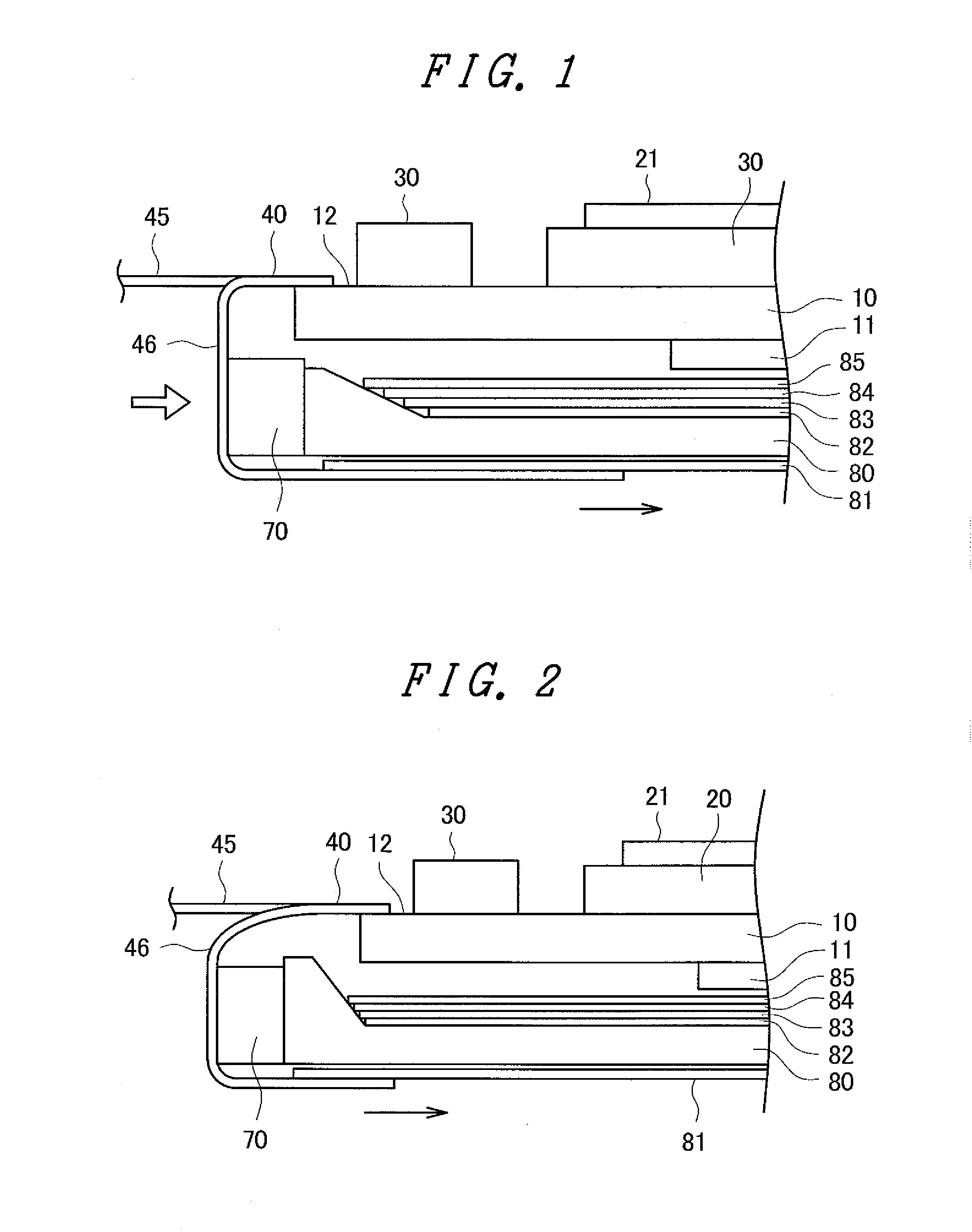
[0058]The embodiment 1 is directed to an example which enhances the utilization efficiency of light emitted from light emitting diodes 70 by improving the close contact between the light emitting diodes 70 and an edge portion of a light guide plate 80. FIG. 1 is a cross-sectional view of a liquid crystal display device showing the embodiment 1 of the present invention. In FIG. 1, the edge portion of the light guide plate 80 is present in the vicinity of an edge portion of a TFT substrate 10.

[0059]In FIG. 1, a flexible printed circuit board 40 is connected to a terminal portion 12 of the TFT substrate 10. With respect to this flexible printed circuit board 40, a light-emitting-diode-use flexible printed circuit board 46 which supplies electricity and the like to the light emitting diodes 70 is folded and extends to and along a back surface of a liquid crystal display panel and a back surface of a backlight. In FIG. 1, a main flexible printed circuit board 45 on which electronic parts...

embodiment 2

[0065]This embodiment provides the constitution which can reduce a thickness of the liquid crystal display device. FIG. 2 is a cross-sectional view showing the constitution of this embodiment. In FIG. 2, a portion of a light guide plate 80 in the vicinity of an edge portion of the light guide plate 80 which faces light emitting diodes 70 has a large plate thickness. Further, the portion is positioned outside an edge portion of a TFT substrate 10. The light emitting diodes 70 are arranged to be in close contact with the edge portion of the light guide plate 80.

[0066]The light emitting diodes 70 require a predetermined height. The edge portion of the light guide plate 80 which faces the light emitting diodes 70 also requires a height substantially equal to the height of the light emitting diodes 70. As shown in FIG. 7, when the light emitting diodes 70 or the edge portion of the light guide plate 80 which faces the light emitting diodes 70 are arranged below the TFT substrate 10, a th...

embodiment 3

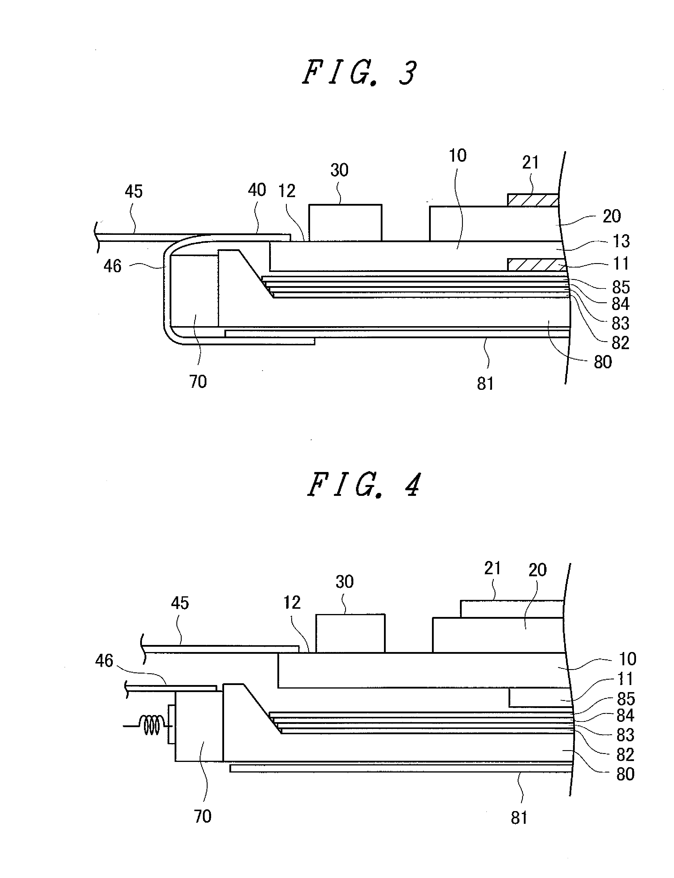
[0069]FIG. 3 is a cross-sectional view of a liquid crystal display device showing an embodiment 3 of the present invention. In the embodiment 2, as shown in FIG. 2, the thickness of the whole liquid crystal display device is reduced by arranging the light emitting diodes 70 and the edge portion of the light guide plate 80 outside the TFT substrate 10. In the constitution of the embodiment 2, as shown in FIG. 2, parts of the liquid crystal display device which define the thickness of the whole liquid crystal display device are the light guide plate 80, the group of optical sheets which is placed on the light guide plate 80, the lower polarizer 11, the TFT substrate 10, the color filter substrate 20, and the upper polarizer 21.

[0070]According to the embodiment 3 shown in FIG. 3, a stepped portion is formed on the TFT substrate 10. That is, while a plate thickness of a portion of the TFT substrate 10 corresponding to the terminal portion 12 is maintained as it is, a plate thickness of ...


PUM


Abstract

A small-sized liquid crystal display device which can enhance light utilization efficiency of light emitting diodes and also can reduce a thickness of the liquid crystal display device is provided. A flexible printed circuit board is connected to a terminal portion of a TFT substrate. In such a flexible printed circuit board, a light-emitting-diode-use flexible printed circuit board is folded and extends toward a back surface of a backlight. Light emitting diodes are arranged on the light-emitting-diode-use flexible printed circuit board in such a manner that the light emitting diodes are pressed against an edge portion of the light guide plate. Since the light emitting diodes and the edge portion of the light guide plate are brought into close contact with each other, the utilization efficiency of light from the light emitting diodes is enhanced. Further, since the light emitting diodes and the edge portion of the light guide plate which faces the light emitting diodes are provided outside the TFT substrate, a thickness of the whole liquid crystal display device can be reduced.

Description

CLAIM OF PRIORITY[0001]The present application claims priority from Japanese application serial No. 2008-281569, filed on Oct. 31, 2008, the content of which is hereby incorporated by reference into this application.BACKGROUND OF THE INVENTION[0002]1. Field of the Invention[0003]The present invention relates to a display device, and more particularly to a liquid crystal display device which is small-sized and can reduce a thickness thereof.[0004]2. Description of the Related Art[0005]A liquid crystal display device includes a thin film transistors (TFT) substrate on which pixel electrodes, TFT and the like are formed in a matrix array, a color filter substrate which faces the TFT substrate in an opposed manner and forms color filters and the like thereon at positions corresponding to the pixel electrodes formed on the TFT substrate, and liquid crystal which is sandwiched between the TFT substrate and the color filter substrate. An image is formed by controlling optical transmissivit...

Claims


Application Information

Patent Timeline
IPC IPC(8): G02F1/1333
CPCG02B6/0083G02B6/0091G02F1/13452G02F2202/28H05K1/189H05K2201/056H05K2201/10106H05K2201/10128
Inventor TATEBAYASHI, YOSHITAKAHOSAKA, AKIRA
Owner PANASONIC LIQUID CRYSTAL DISPLAY CO LTD
Why Eureka
Try Eureka