Light emitting diode, production method thereof and lamp

Inactive Publication Date: 2010-05-20
SHOWA DENKO KK
View PDF0 Cites 12 Cited by
  • Summary
  • Abstract
  • Description
  • Claims
  • Application Information

AI Technical Summary

Benefits of technology

[0033]With the light emitting diode according to the invention; since the first electrode formed on the compound semiconductor layer includes the wiring electrode provided on the compound semiconductor layer in contact therewith, the ohmic electrode provided on the compound semiconductor layer in contact therewith, the translucent electrode formed over the compound semiconductor layer to cover the wiring electrode and the ohmic electrode, and the bonding pad electrode connected to the wiring electrode, at least a portion of the bonding pad electrode being exposed from an opening of the translucent electrode to the exterior; it is possible to subject the surface of the compound semiconductor layer having the light emitting layer to a roughening process; so that the light extraction efficiency from the light emitting layer is enhanced; and the high luminance is achieved. Also, since the translucent electrode protects th

Problems solved by technology

For this reason, there is a problem in that an electric current is introduced into only a region of the compound semiconductor layer immediately below an electrode and thus the light emitted from the light emitting layer is blocked by the electrode, so that the light could not be emitted to the outside.
First, in the case where the metal electrode is formed on the translucent electrode, when the surface of the semiconductor layer is processed to become rough state for the purpose of enhancing the light extraction efficiency, the adhesion strength between the metal electrode and the translucent electrode is likely to be deteriorated or the metal electrode is likely to be disconnected.
T

Method used


Image

  • Light emitting diode, production method thereof and lamp
  • Light emitting diode, production method thereof and lamp
  • Light emitting diode, production method thereof and lamp

Examples


example 1

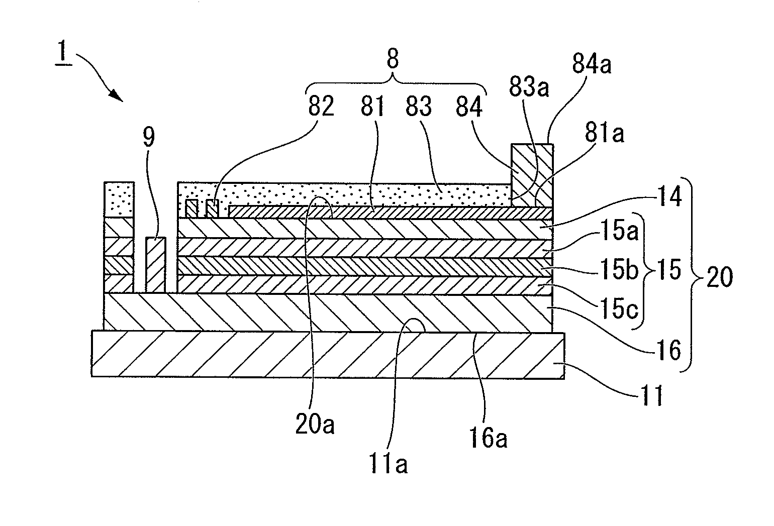
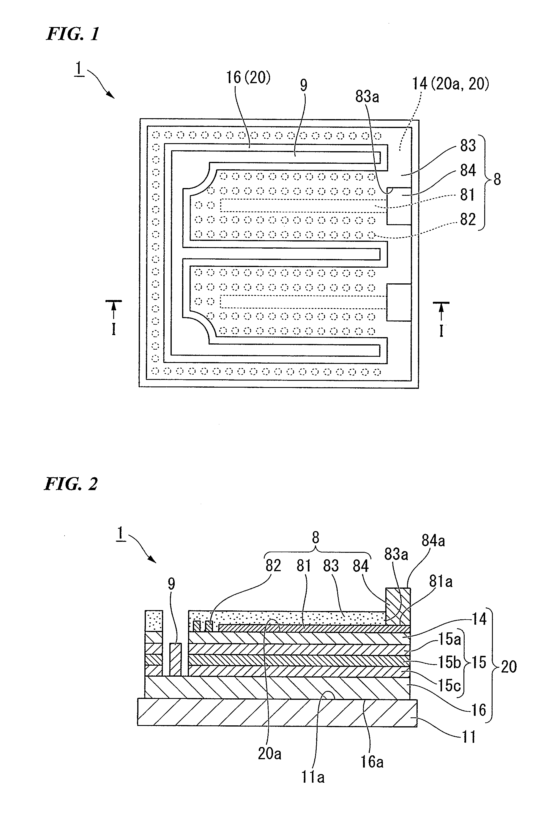
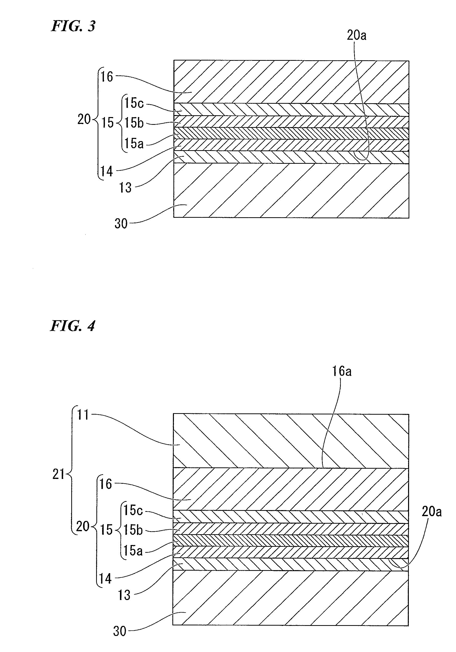
[0166]FIGS. 1 and 2 are views schematically showing a light emitting diode produced according to an example. FIG. 1 is a plan view of the light emitting diode, and FIG. 2 is a cross-sectional view taken along the line I-I in FIG. 1. FIGS. 3 and 4 are cross-sectional views schematically showing a layer structure of a semiconductor stacked wafer. FIGS. 5A to 5D are process views showing a process of forming an n-type electrode (first electrode) on a compound semiconductor layer. FIGS. 6 and 7 are cross-sectional views schematically showing a lamp produced by using the light emitting diode shown in FIG. 1.

[0167]In the example, an epitaxially stacked structure (a semiconductor stacked wafer) formed on a substrate for epitaxial growth made of GaAs was bonded onto a substrate made of GaP to produce a light emitting diode emitting red light and having a light emitting layer made of AlGaInP-based compound semiconductor. Further, a top view-type lamp was produced by using the light emitting ...

example 2

[0209]In this example, a light emitting diode 2 was produced in the same method as that of the example 1, as shown in FIGS. 8A to 8C, except that a p-type electrode 19 was formed on a rear surface 12b of a substrate 12 made of GaP to form a vertical electrode structure.

[0210]Bonding of Substrate

[0211]In this example, a substrate 12 which is a p-type GaP single-crystal substrate was bonded onto a p-type semiconductor layer 16 (surface 16a) of a compound semiconductor layer 20 formed in the same order as that of the example 1. The substrate 12 added with Zn to have the carrier concentration of approximately 1×1018 cm−3 and having q (100) crystal plane orientation was a p-type single-crystal substrate, and the substrate having a diameter of approximately 50 mm and a thickness of approximately 250 μm was prepared. Also, the substrate 12 had a surface roughness of approximately 0.11 nm which is a value of a root mean square (RMS), by subjecting a main surface 12a to mirror polishing.

[021...


PUM


Abstract

A light emitting diode includes a substrate, a compound semiconductor layer including a light emitting layer formed on the substrate, a first electrode formed on an upper surface of the compound semiconductor layer, and a second electrode formed on the substrate or a semiconductor layer which is exposed by removing at least a portion of the compound semiconductor layer. The first electrode includes a wiring electrode provided on the compound semiconductor layer in contact therewith, an ohmic electrode provided on the compound semiconductor layer in contact therewith, a translucent electrode formed over the compound semiconductor layer to cover the wiring electrode and the ohmic electrode, and a bonding pad electrode connected to the wiring electrode, at least a portion of the bonding pad electrode being exposed from an opening of the translucent electrode to the exterior.

Description

CROSS REFERENCE TO RELATED APPLICATIONS[0001]Priority is claimed on Japanese Patent Application No. 2008-295827, filed Nov. 19, 2008.BACKGROUND OF THE INVENTION[0002]1. Field of the Invention[0003]The present invention relates to a light emitting diode with a compound semiconductor layer stacked on a substrate, a production method thereof and a lamp.[0004]2. Description of Related Art[0005]As a light emitting diode (LED) capable of emitting a visible light of a red color, an orange color, a yellow color or a yellowish-green color; a compound semiconductor LED that is equipped with a light emitting layer formed of an aluminum-gallium-indium phosphide ((AlXGa1-X)YIn1-YP in which (0≦X≦1, 0<Y≦1)) has been hitherto known. In LEDs of this kind, a compound semiconductor layer having a light emitting layer made of (AlXGa1-X)YIn1-YP in which (0≦X≦1, 0<Y≦1) is generally formed on a substrate material, such as gallium arsenide (GaAs) which is optically opaque to the light emitted from th...

Claims


Application Information

Patent Timeline
IPC IPC(8): H01L33/00
CPCH01L33/22H01L33/387H01L33/42H01L2224/48091H01L2224/73265H01L2924/00014
Inventor TAKEUCHI, RYOUICHIMASUYA, KYOUSUKE
Owner SHOWA DENKO KK
Why Eureka
Try Eureka