Compound and organic electroluminescent device using same

Inactive Publication Date: 2007-05-31
CANON KK
View PDF18 Cites 22 Cited by
  • Summary
  • Abstract
  • Description
  • Claims
  • Application Information

AI Technical Summary

Benefits of technology

[0025] The light-emitting device of the present invention using the compound of the present invention for a host of a light-emitting layer is an excellent device capable of emitting light with a high efficiency and maintaining a high luminance for a

Problems solved by technology

In addition, there still remain a large number of problems in terms of durability such as a change over time due to long-term use and deterioration due to an atmospheric gas containing oxygen or to moisture.
However, those proble

Method used


Image

  • Compound and organic electroluminescent device using same
  • Compound and organic electroluminescent device using same
  • Compound and organic electroluminescent device using same

Examples


example 1

Synthesis of Exemplified Compound No. X-25

[0075]

[0076] 1 g (1.35 mmole) of Compound A, 672 mg (3.39 mmole) of 2-biphenylboric acid, 156 mg of Pd(PPh3)4, 20 ml of toluene, 10 ml of ethanol, and 20 ml of a 2M aqueous solution of sodium carbonate were fed into a 100-ml round-bottomed flask, and the whole was stirred at 80° C. for 8 hours in a stream of nitrogen. After the completion of the reaction, the resultant was extracted with toluene, and the organic layer was dried with magnesium sulfate. After that, the drying agent was filtered and the solvent was distilled off. The residue was dissolved into chloroform, and the solution was separated and purified by means of alumina column chromatography, followed by .recrystallization from toluene. The resultant crystal was vacuum-dried at 120° C., and the resultant was sublimated and purified to give 700 mg of Exemplified Compound No. X-25 (58% yield).

[0077] 882.4 as M+ of the compound was confirmed by means of Matrix Assisted Laser Desorp...

example 2

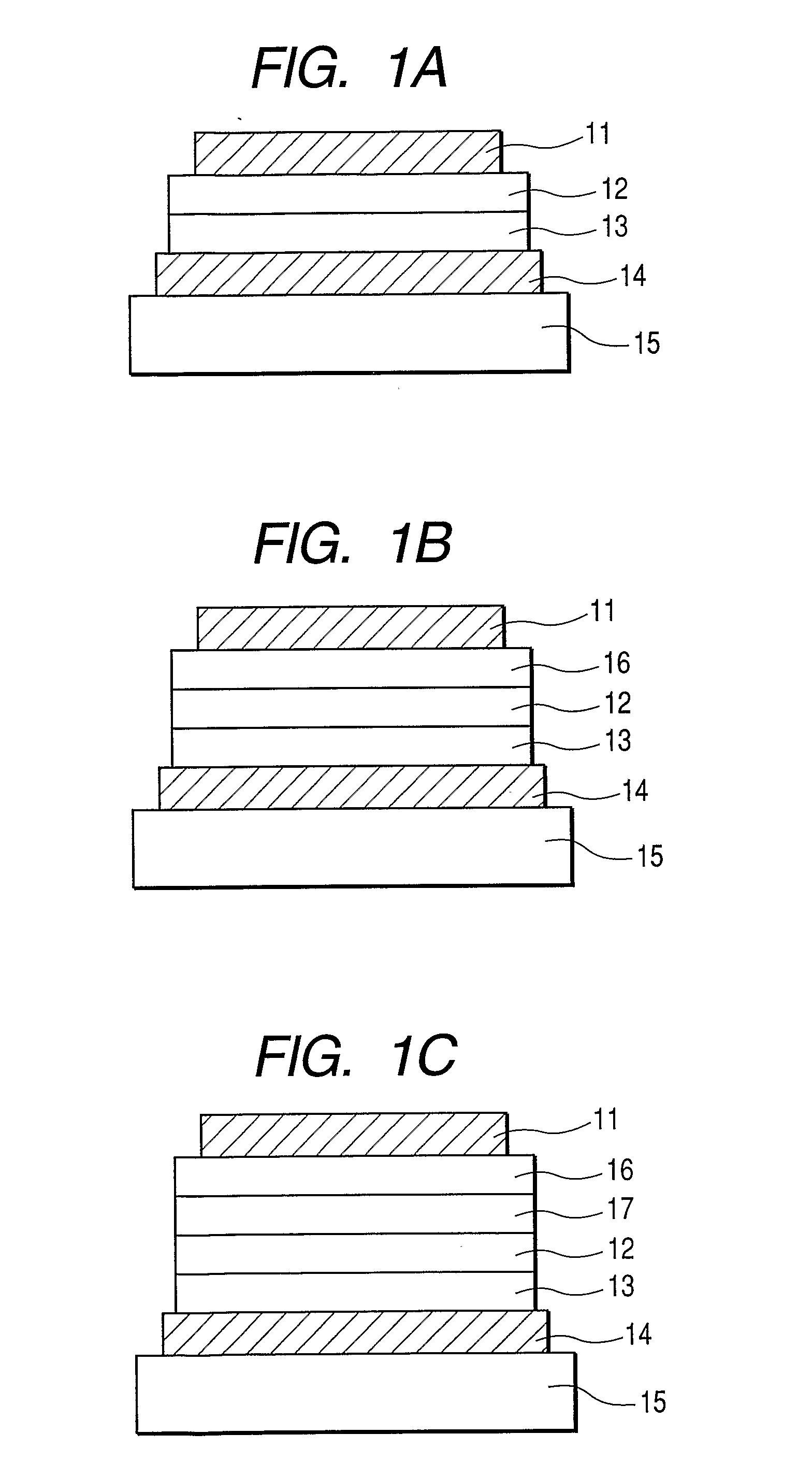
[0081] In this example, a device having three organic layers shown in FIG. 1B was used as a device structure.

[0082] ITO (as the transparent electrode 14) having a thickness of 100 nm was patterned on a glass substrate (as the transparent substrate 15). The following organic layers and electrode layers were successively formed on the ITO substrate by means of vacuum evaporation according to resistive heating .in a vacuum chamber having a pressure of 10−5 Pa such that the opposing electrode area was 3 mm2. Hole-transporting layer 13 (50 nm): α-NPD Light-emitting layer 12 (50 nm): [Host] Exemplified Compound No. X-25, [Guest] Ir(4mopiq)3 (weight ratio: 4%) and Ir(bq)3 (weight ratio: 8%) Electron-transporting layer 16 (50 nm): Bphen (manufactured by DOJINDO LABORATORIES) Metal electrode layer 1 (1 nm): KF Metal electrode layer 2 (130 nm): Al

[0083] The current-voltage characteristics of the EL device were measured by using a microammeter 4140B (manufactured by Hewlett-Packard Developme...

example 3

Synthesis of Exemplified Compound No. X-23

[0090]

[0091] 2 g (3.13 mmole) of Compound B, 1.38 g (6.89 mmole) of 2-bromophenylboric acid, 400 mg of Pd(PPh3)4, 20 ml of toluene, 10 ml of ethanol, and 20 ml of a 2M aqueous solution of sodium carbonate were fed into a 100-ml round-bottomed flask, and the whole was stirred at 80° C. for 4 hours in a stream of nitrogen. After the completion of the reaction, the resultant was extracted with toluene, and the organic layer was dried with magnesium sulfate. After that, the drying agent was filtered and the solvent was distilled off. The residue was dissolved into chloroform, and the solution was separated and purified by means of silica gel chromatography, followed by recrystallization from toluene, to thereby give 1.37 g of Compound C (63% yield).

[0092] 694.1 as M+ of the compound was observed by means of Matrix Assisted Laser Desorption / Ionization-Time of Flight Mass Spectrometry (MALDI-TOF MS).

[0093] In addition, the structure of the compo...


PUM

PropertyMeasurementUnit
Temperatureaaaaaaaaaa

Abstract

Provided is a novel compound that can be suitably used as a compound for an organic EL device. The compound is represented by general formula (1):
wherein x, y and z are an integer of 0 to 3 with x+z>1;
R3, R15, R16, R17, and R18 are hydrogen or a linear or branched alkyl;
R1, R2, R4, and R5 are hydrogen, a linear or branched alkyl, or a substituted or unsubstituted aryl with at least one being a substituted or unsubstituted aryl;
A is hydrogen, a linear or branched alkyl, or group B:
(wherein R6, R7, R8, R9, and R10 are hydrogen, a linear or branched alkyl, or a substituted or unsubstituted aryl);
R11, R12, R13, and R14 are hydrogen, a linear or branched alkyl, or a substituted or unsubstituted aryl; and each CH on the benzene ring may be replaced by nitrogen.

Description

TECHNICAL FIELD [0001] The present invention relates to a light-emitting device using an organic compound, and more particularly to a novel compound having a specific molecular structure and an organic electroluminescent (EL) device using the same. BACKGROUND ART [0002] In an old example of an organic light-emitting device, a voltage is applied to an anthracene evaporated film to emit light (Thin Solid Films, 94 (1982), 171). In addition, applied research on an organic light-emitting device has been vigorously conducted. [0003] As detailed in Macromol. Symp. 125, 1 to 48 (1997), an organic EL device is generally, structured to have two (upper and lower) electrodes formed on a transparent substrate and an organic substance layer including a light-emitting layer formed between the electrodes. [0004] In addition, investigation has been recently made into a device using not only conventional light emission utilizing fluorescence upon transition from singlet exciton to ground state but a...

Claims


Application Information

Patent Timeline
IPC IPC(8): H01L51/54C07C13/567C09K11/06
CPCC07C13/567C07C22/08C07C25/13C09K11/06C09K2211/1007C09K2211/1011C09K2211/1029C09K2211/1044C09K2211/182C09K2211/185C09K2211/186C09K2211/188H05B33/14H10K85/115H10K85/111H10K85/151H10K50/11
Inventor HASHIMOTO, MASASHIOKADA, SHINJIROTAKIGUCHI, TAKAOKAMATANI, JUNIQAWA, SATOSHINAKASU, MINAKOIWAWAKI, HIRONOBUOOISHI, RYOTA
Owner CANON KK
Why Eureka
Try Eureka