Step attenuator circuit with improved insertion loss

a step attenuator and insertion loss technology, applied in the field of electronic filters, can solve the problems of increasing the insertion loss of the step attenuator, affecting performance, and affecting the performance of the attenuator, and achieve the effect of reducing costs

Inactive Publication Date: 2010-06-03
TRESNESS 2013 IRREVOCABLE PATENT TRUST
View PDF7 Cites 5 Cited by
  • Summary
  • Abstract
  • Description
  • Claims
  • Application Information

AI Technical Summary

Benefits of technology

[0017]In the preferred embodiment, first and second capacitive circuits each consists of a single capacitor, because the use of one capacitor is usually sufficient, requires the least amount of area on a printed circuit board, and minimizes cost.

Problems solved by technology

As signal frequencies approach 1000 MHz and higher, the parasitic capacitance in a step attenuator circuit begins to adversely affect performance.
This lost power manifests itself in the form of a higher insertion loss for the step attenuator, and is particularly noticeable at ultra high frequencies (UHF) above 750 MHz.
Thus, there is little room for separating circuit components and board traces in current step attenuator packages.
Thus, the shielding technique may not be an optimum solution, and would likely add to the cost of manufacturer.
The use of ground planes (e.g., sandwiched between layers of printed circuit board) to reduce parasitic capacitance may also add to the cost and complexity of manufacture and produce unintended stray capacitance, resulting in frequency response roll-off.

Method used


Image

  • Step attenuator circuit with improved insertion loss
  • Step attenuator circuit with improved insertion loss
  • Step attenuator circuit with improved insertion loss

Examples


Embodiment Construction

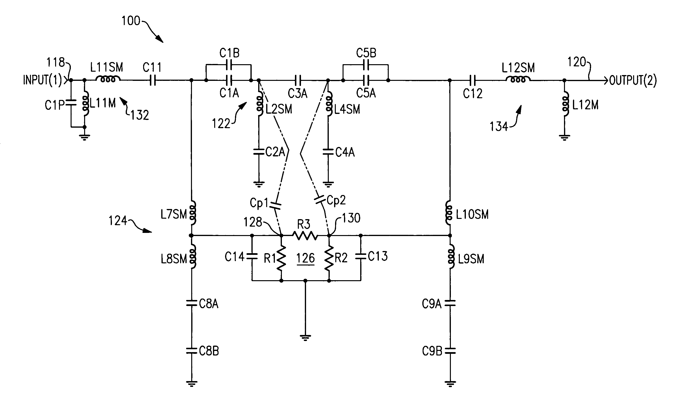
[0030]FIG. 3 shows a schematic diagram of a preferred embodiment of a step attenuator circuit 100, constructed in accordance with the present invention. Circuit 100 comprises an input line 118, an output line 120, a highpass filter network 122, a lowpass filter network 124, and an attenuator network 126 forming part of lowpass network 124. Highpass network 122 is an elliptic-function filter, consisting of: capacitors C1B, C1A, C2A, C3A, C4A, C5A, and C5B; and inductors L2SM and L4SM. Lowpass network 124 is an elliptic-function filter, consisting of: inductors L7SM, L8SM, L9SM, and L10SM; capacitors C8A, C8B, C9A, and C9B; and attenuator network 126. In this preferred embodiment, attenuator network 126 is a resistive Pi network, consisting of resistors R1, R2 and R3. Attenuator network 126 has an input node 128 and an output node 130.

[0031]The values of the capacitors and inductors of highpass network 122 are determined so that network 122 passes high frequency signals from 54-1000 M...


PUM


Abstract

A step attenuator circuit is mounted on a printed circuit board and has a highpass filter network passing high frequency signals and a lowpass filter network passing low frequency signals. The lowpass network presents a high shunt reactance to the high frequency signals. The lowpass network includes an attenuator network. The attenuator network attenuates the low frequency signals by a specified amount. Parasitic capacitance exists between the highpass network and the attenuator network, causing an amount of electrical energy from the high frequency signals to be absorbed by the attenuator network. A first capacitive circuit is used to compensate for parasitic capacitance. The first compensation circuit is connected across the attenuator network and is coupled to the parasitic capacitance. Consequently, the amount of electrical energy from the high frequency signals absorbed by the attenuator network is reduced, and, as a result, the insertion loss of the step attenuator is reduced.

Description

BACKGROUND OF THE INVENTION[0001]The present invention relates generally to electronic filters for processing communication signals, and more particularly to an electronic filter called a step attenuator and a circuit modification for improving the insertion loss of the step attenuator.[0002]A step attenuator is a filter used primarily (but not exclusively) in a bi-directional cable television (or CATV) network. The step attenuator is also bi-directional. It processes signals transmitted from a headend to a subscriber's home (i.e., “forward path”) and also processes signals transmitted from the subscriber's home to the headend (i.e., “return path”). Usually, the forward path signals are transmitted in a higher frequency band than the return path signals. In the United States, for example, the forward path frequency band is 54-1000 MHz and the return path band is 5-42 MHz. A step attenuator is usually installed in the CATV network at a subscriber tap port, just upstream of the subscr...

Claims


Application Information

Patent Timeline
Patent Type & Authority Applications(United States)
IPC IPC(8): H03H7/00
CPCH03H7/0115H03H7/38H03H7/24H03H7/1758
Inventor ZELENZ, MARTIN L.
Owner TRESNESS 2013 IRREVOCABLE PATENT TRUST
Why Eureka
Try Eureka