Printed circuit board having plating pattern buried in via and method of manufacturing the same

a technology of printed circuit boards and vias, which is applied in the direction of resistive material coating, railway components, nuclear engineering, etc., can solve the problems of reducing the production efficiency of pcb, so as to reduce the generation of pcb deviations.

Inactive Publication Date: 2010-06-10
SAMSUNG ELECTRO MECHANICS CO LTD
View PDF7 Cites 15 Cited by
  • Summary
  • Abstract
  • Description
  • Claims
  • Application Information

AI Technical Summary

Benefits of technology

[0015]Accordingly, the present invention has been made keeping in mind the problems encountered in the related art and the present invention provides a PCB which is constructed such tha...

Problems solved by technology

However, as the circuit of a PCB such as a semiconductor substrate becomes finer, the ability to use a subtractive process to form a fine circuit becomes exceeded.
However, in the case where the circuit layer is formed through SAP or MSAP, the size of the pad of the via 19 is increased, thus making it difficult to realize a fine circuit.
Also...

Method used


Image

  • Printed circuit board having plating pattern buried in via and method of manufacturing the same
  • Printed circuit board having plating pattern buried in via and method of manufacturing the same
  • Printed circuit board having plating pattern buried in via and method of manufacturing the same

Examples


Embodiment Construction

[0032]Hereinafter, a detailed description will be given of a PCB having a plating pattern buried in a via and a manufacturing method thereof according to the present invention, with reference to the appended drawings. Throughout the drawings, the same reference numerals refer to the same or similar elements, and redundant descriptions are omitted. In the description, the terms “upper”, “lower” and so on are used only to distinguish one element from another element, and the elements are not defined by the above terms.

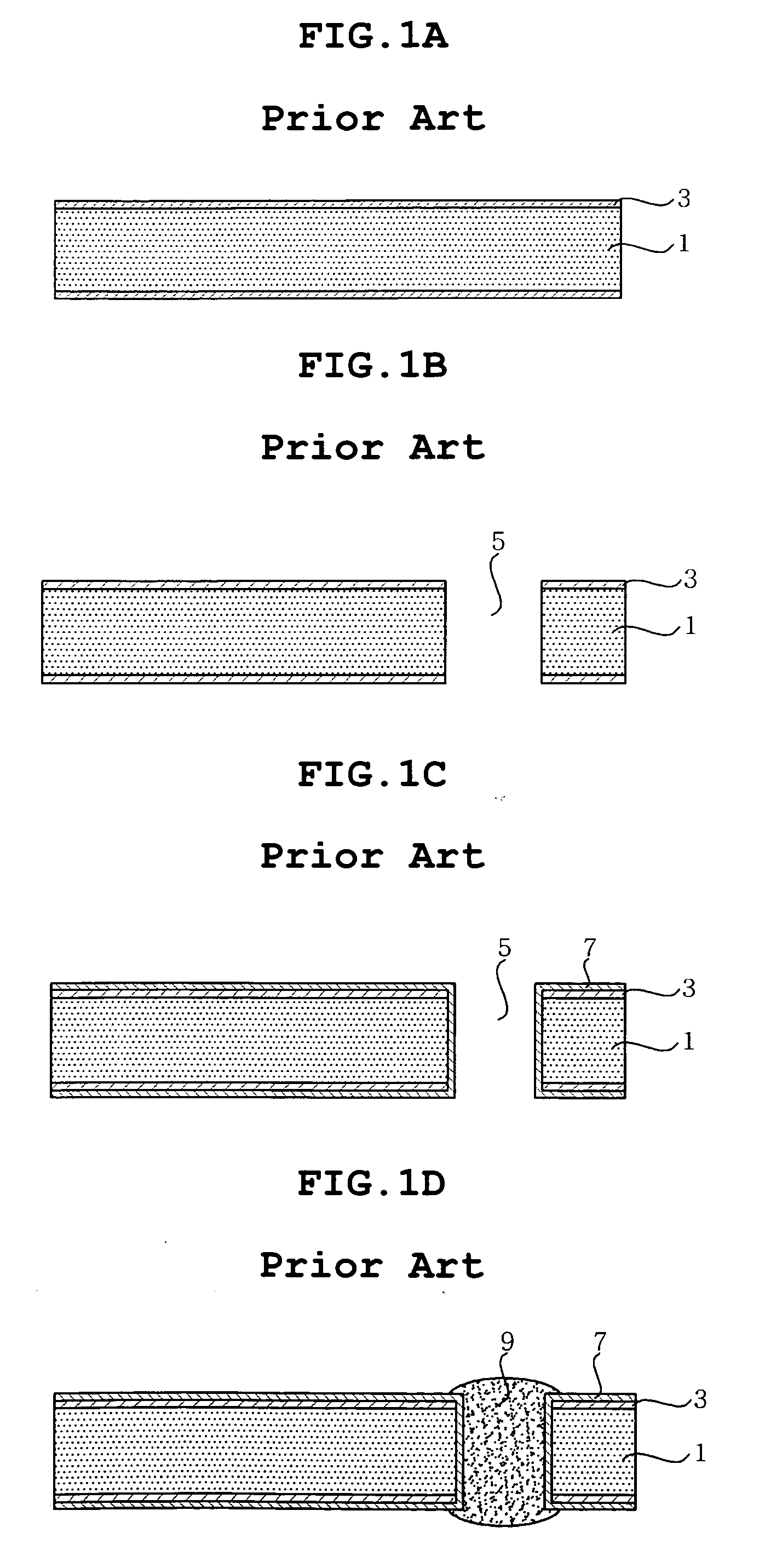
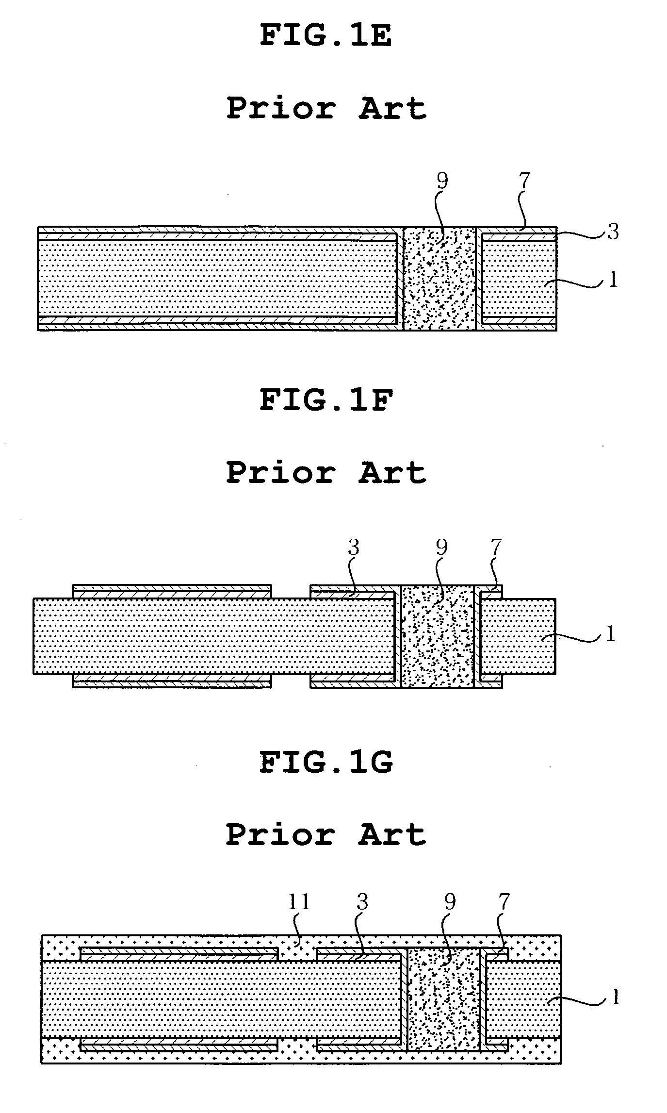
[0033]FIGS. 2 to 9 sequentially show the process of manufacturing the PCB having a plating pattern buried in a via according to an embodiment of the present invention.

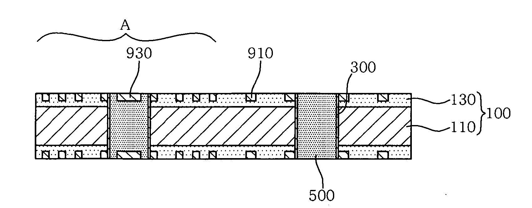
[0034]First, an insulating substrate 100 is provided, and via holes 150 are formed in the insulating substrate 100.

[0035]As shown in FIG. 2, an insulating substrate 100 is prepared. The insulating substrate 100 used in the present invention includes a core substrate 110 made of a glass fiber-reinforced ther...


PUM

PropertyMeasurementUnit
Thicknessaaaaaaaaaa
Densityaaaaaaaaaa
Heightaaaaaaaaaa

Abstract

Disclosed is a printed circuit board having a plating pattern buried in a via and a method of manufacturing the same. The method of manufacturing the printed circuit board includes forming a negative pattern for forming a plating pattern, thus remarkably reducing the generation of plating thickness deviation in a plating process for forming a circuit pattern, and the printed circuit board has improved electrical signal transmission properties.

Description

CROSS REFERENCE TO RELATED APPLICATION[0001]This application claims the benefit of Korean Patent Application No. 10-2008-0124153, filed Dec. 8, 2008, entitled “A printed circuit board comprising a plating-pattern buried in via and a method of manufacturing the same”, which is hereby incorporated by reference in its entirety into this application.BACKGROUND OF THE INVENTION[0002]1. Field of the Invention[0003]The present invention relates to a printed circuit board (PCB) having a plating pattern buried in a via and a method of manufacturing the same, and, more particularly, to a method of manufacturing a PCB, which includes forming a negative pattern for forming a plating pattern, thus remarkably reducing the generation of plating thickness deviation in a plating process for forming a circuit pattern, and to a PCB having improved electrical signal transmission properties.[0004]2. Description of the Related Art[0005]With the advancement of the electronics industry, the demand for incr...

Claims


Application Information

Patent Timeline
IPC IPC(8): H05K1/00H05K1/11
CPCH05K2201/0959H05K3/045Y10T29/49144H05K2203/025H05K3/0032H05K2203/1461Y10T29/49165Y10T29/49117H05K3/107H05K2201/0376H05K3/426Y10T29/49126Y10T29/4913H05K3/40H05K3/42H05K3/18
Inventor AHN, SEOK HWANKO, YOUNG GWAN
Owner SAMSUNG ELECTRO MECHANICS CO LTD
Why Eureka
Try Eureka