Organic light emitting display device and method of driving the same

a technology of light-emitting display and organic light-emitting device, which is applied in the direction of semiconductor devices, instruments, computing, etc., can solve the problem of inability to display images with even brightness

Active Publication Date: 2010-06-10
SAMSUNG DISPLAY CO LTD
View PDF8 Cites 40 Cited by
  • Summary
  • Abstract
  • Description
  • Claims
  • Application Information

AI Technical Summary

Benefits of technology

[0021]With the organic light emitting diode and the method of driving the same according to the present invention, the amount of current flowing onto the organic light emitting diode is determined regardless of the threshold voltage of the transistor, making it possible to display images having an even brightness. Also, image having a desired brightness can be displayed by compensating for characteristic deviation of the transistor.

Problems solved by technology

However, the conventional organic light emitting display device as above has a problem that images having even brightness cannot be displayed due to deviation of threshold voltage.

Method used


Image

  • Organic light emitting display device and method of driving the same
  • Organic light emitting display device and method of driving the same
  • Organic light emitting display device and method of driving the same

Examples


first embodiment

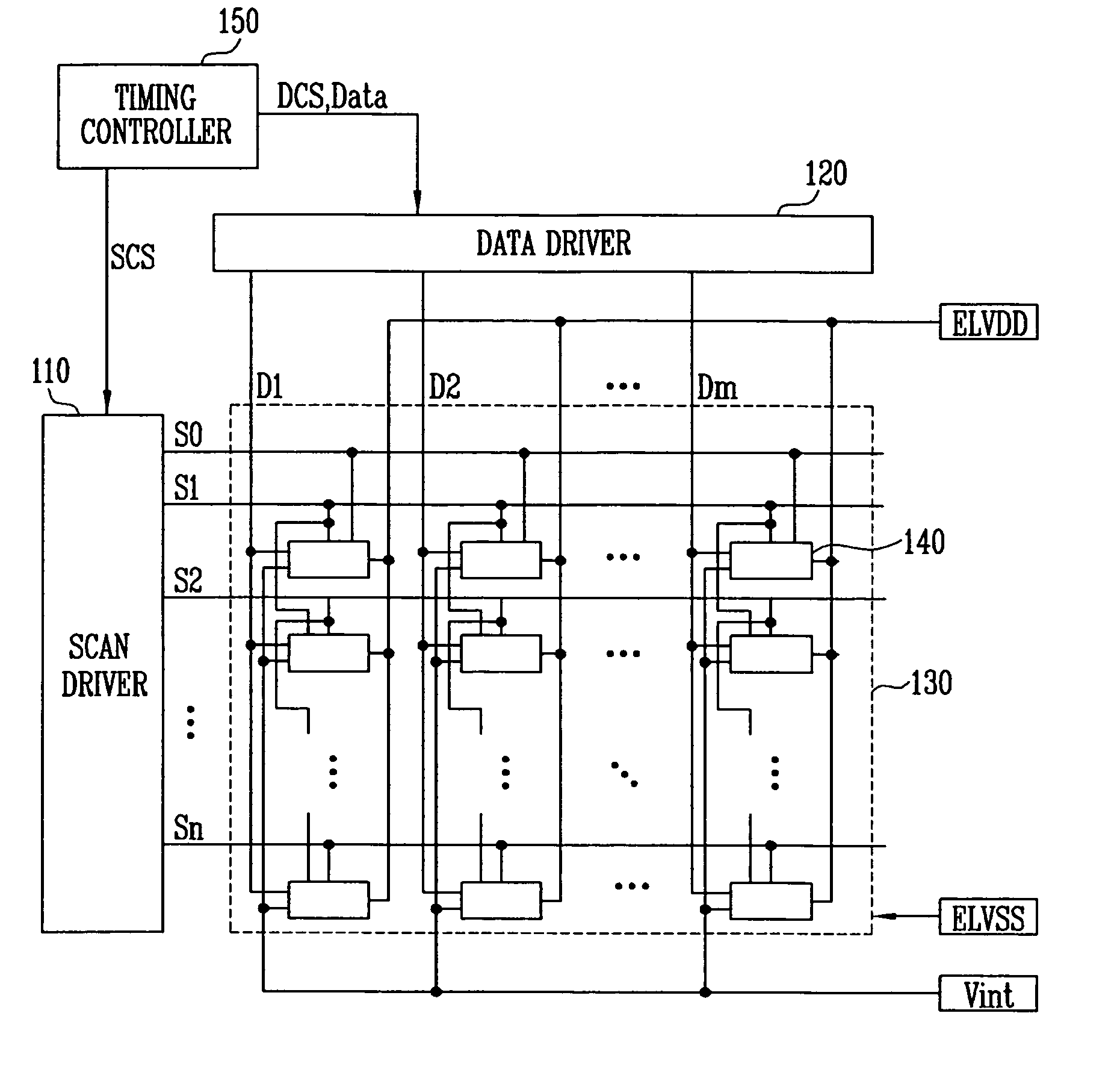
[0039]FIG. 3 shows the pixel 140 of FIG. 2. For convenience of explanation, a pixel 140 is positioned in an nth horizontal line and connected to an mth data line Dm will be described.

[0040]Referring to FIG. 3, the pixel 140, according to the first embodiment, includes an organic light emitting diode OLED and a pixel circuit 142 connected to a data line Dm and scan lines Sn-1 and Sn to control the organic light emitting diode OLED.

[0041]An anode electrode of the organic light emitting diode OLED is connected to the pixel circuit 142, and a cathode electrode thereof is connected to a second power supply ELVSS. The organic light emitting diode OLED as above generates light having a predetermined brightness, corresponding to current supplied from the pixel circuit 142.

[0042]The pixel circuit 142 is charged with a voltage corresponding to a data signal supplied to the data line Dm when a scan signal is supplied to the scan line Sn and voltage corresponding to threshold voltage of a first...

second embodiment

[0066]FIG. 5 shows the pixel of FIG. 2. When describing FIG. 5, the same reference numerals will be given to the same constitution of FIG. 3 and the detailed description thereof will be omitted.

[0067]Referring to FIG. 5, the pixel according to the second embodiment includes an organic light emitting diode OLED and a pixel circuit 142′ connected to a data line Dm and a scan line Sn to control the organic light emitting diode OLED.

[0068]An anode electrode of the organic light emitting diode OLED is connected to the pixel circuit 142′ at node N2, and a cathode electrode thereof is connected to a second power supply ELVSS. The organic light emitting diode OLED as above generates light having a predetermined brightness, corresponding to current supplied from the pixel circuit 142′.

[0069]The pixel circuit 142′ is charged with a voltage corresponding to a data signal supplied to the data line Dm when a scan signal is supplied to the scan line Sn and voltage corresponding to threshold volta...


PUM


Abstract

An organic light emitting display device capable of driving transistor threshold voltage compensation, including: pixels positioned in the intersections of scan lines and data lines, wherein each pixel comprises: a first transistor and a fourth transistor, connected at a common node, disposed between an anode of an OLED and a first power supply; a cathode of the OLED connected to a second power supply; a second transistor connected between a gate of the first transistor and a data line, and turned on when a scan signal is supplied to a scan line; a third transistor connected between the common node and the data line, and turned on when a scan signal is supplied to the scan line; a first capacitor connected between the gate of the first transistor and the anode of the OLED; and a second capacitor connected between the anode of the OLED and a predetermined voltage source.

Description

CROSS REFERENCE TO RELATED APPLICATIONS[0001]This application makes reference to, incorporates the same herein, and claims all benefits accruing under 35 U.S.C §119 from an application entitled ORGANIC LIGHT EMITTING DISPLAY DEVICE AND METHOD OF DRIVING THE SAME earlier filed in the Korean Industrial Property Office on 5 Dec. 2008, which was duly assigned Serial No. 10-2008-0123141 by that Office.BACKGROUND OF THE INVENTION[0002]1. Field of the Invention[0003]The present invention relates to an organic light emitting display device and a method of driving the same, and more particularly to an organic light emitting display device capable of compensating for threshold voltage of a driving transistor and a method of driving the same.[0004]2. Discussion of Related Art[0005]Recently, various flat panel display devices capable of reduced in weight and volume over cathode ray tubes have been developed. As the flat panel display device, there are a liquid crystal display device, a field em...

Claims


Application Information

Patent Timeline
Patent Type & Authority Applications(United States)
IPC IPC(8): G09G5/00G09G3/30
CPCG09G3/3233G09G2300/0819G09G2320/043G09G2300/0861G09G2300/0852H01L21/02576H01L29/742
Inventor CHOI, SANG-MOOLEE, HUN-JUNGKIM, SU-YOUNGCHOI, DONG-WOOK
Owner SAMSUNG DISPLAY CO LTD
Why Eureka
Try Eureka