
Semiconductor die package with clip interconnection

a technology of semiconductor die package and clip, which is applied in the direction of semiconductor/solid-state device details, electrical equipment, semiconductor devices, etc., can solve the problems of difficult clip connection to drain lead 177, semiconductor die package generates a significant amount of heat, and the cost of semiconductor die package production is high

Active Publication Date: 2010-06-17
SEMICON COMPONENTS IND LLC
View PDF9 Cites 13 Cited by
  • Summary
  • Abstract
  • Description
  • Claims
  • Application Information

AI Technical Summary

Benefits of technology

[0059]Embodiments of the invention have a number of advantages. For example, embodiments of the invention are compatible with the footprint of MLP, LFPAK, and S08 type packages, since the thermal drain is at the bottom of the semiconductor die package. Second, the source and gate clip interconnection is a one piece design. The process of interconnecting the gate and source is performed in a single process step (without wirebonding) and only one reflow process needs to be used. In the semiconductor die packages, the gate metal connection can be isolated from a source metal connection after the sawing. Further, the frame design for the leadframe structures has folded tabs, which serve as a location mechanism for a clip frame array during the clip attach process. Also, the clip frame can be a dual gauge frame. The source protruding portion can be at least about twice as thick as the other portions of the clip structure. This provides good heat dissipation from the semiconductor die from both the top and bottom of the die. Lastly, dies of different sizes can be mounted on a die attach pad with a standard foot print.

Problems solved by technology

First, power semiconductor die packages generate a significant amount of heat.
Third, the clip connection to the drain lead 177 is a difficult, because it needs to be bent and aligned with a downset portion of the drain clip 101.
The somewhat complicated structure also makes the semiconductor die package more expensive to produce.
Fourth, the limited amount of space associated with the source die attach pad can limit the size of the dies used in the semiconductor die package.

Method used


Image

  • Semiconductor die package with clip interconnection
  • Semiconductor die package with clip interconnection
  • Semiconductor die package with clip interconnection

Examples


Embodiment Construction

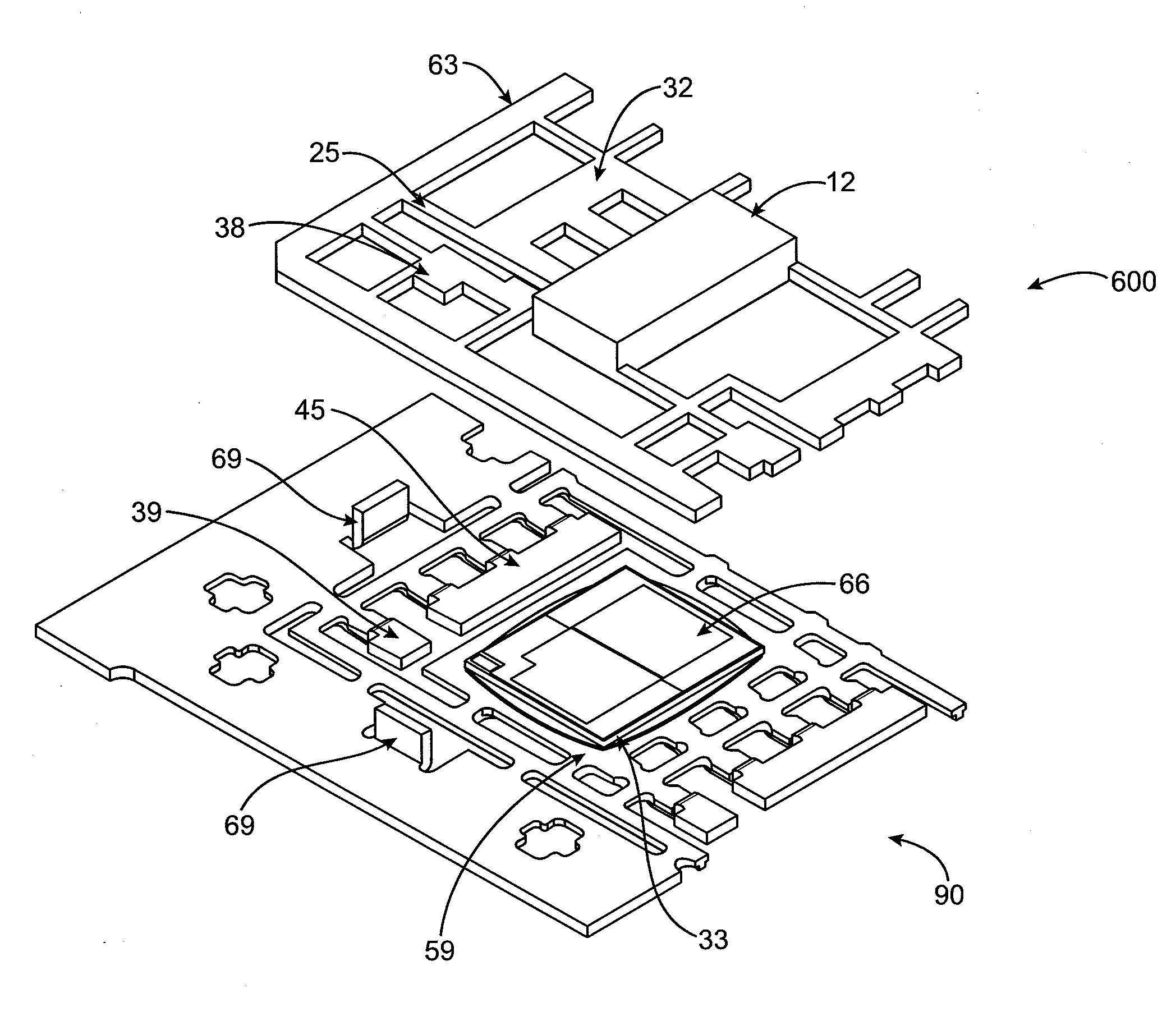
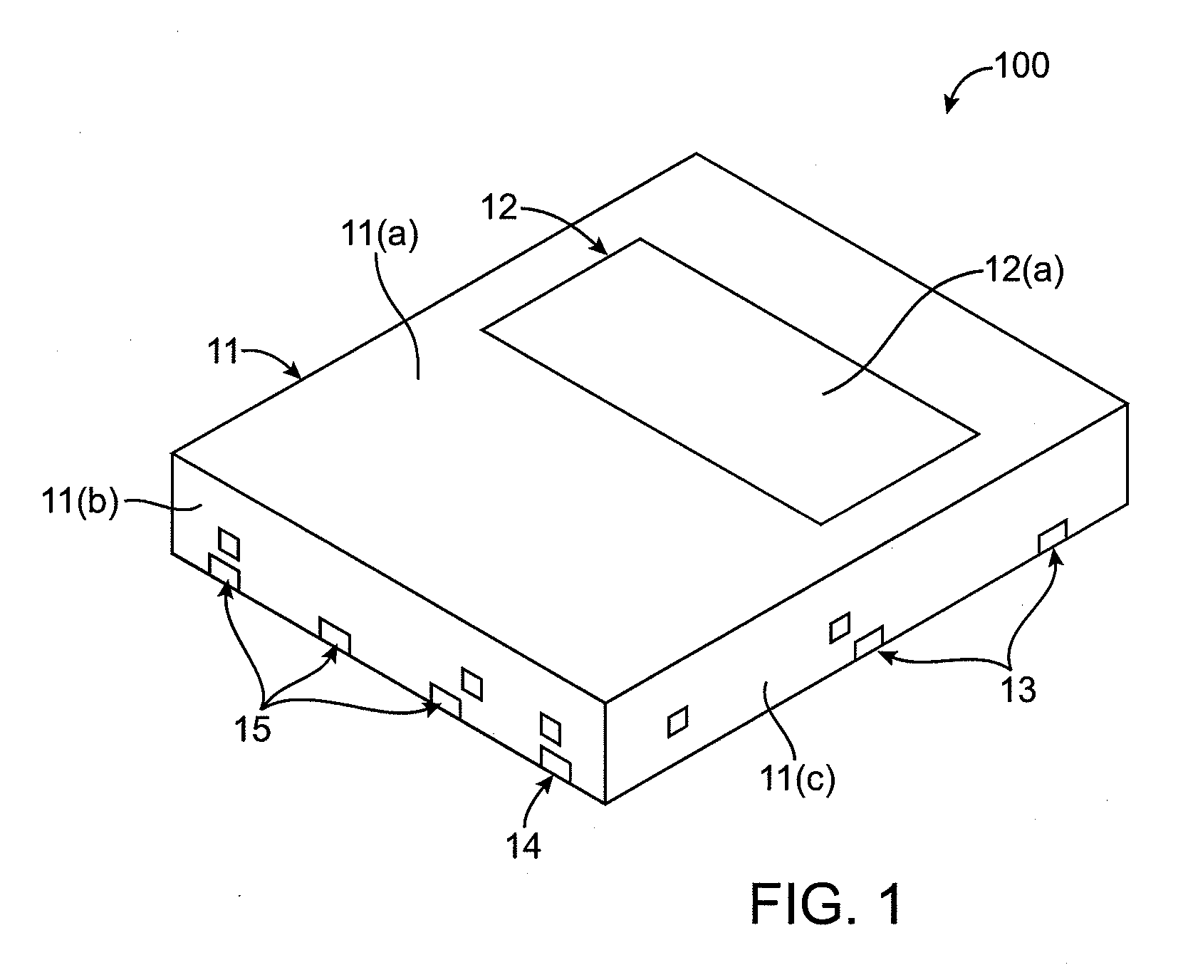
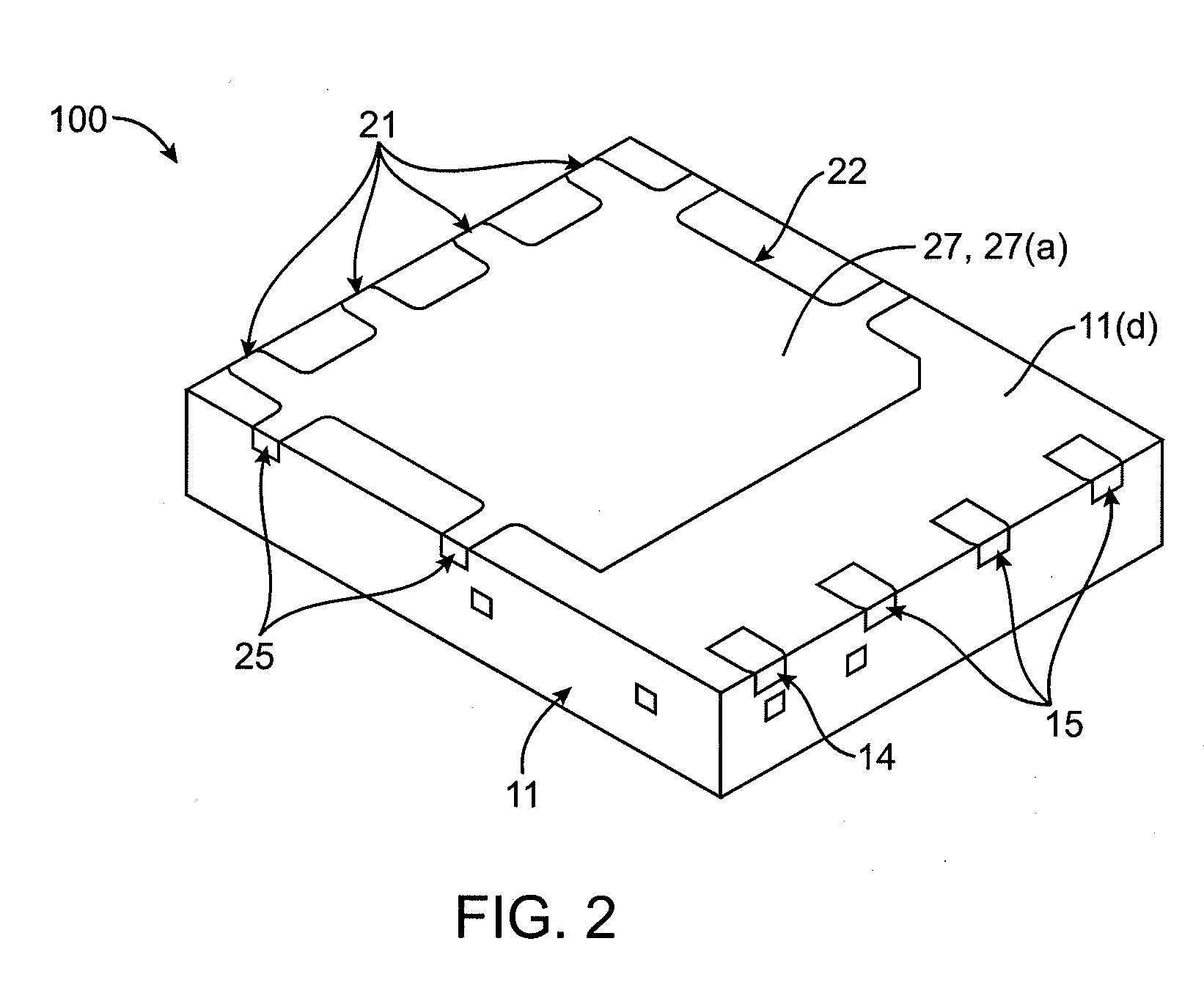
[0027]One embodiment of the invention is directed to a semiconductor die package. The semiconductor die package comprises a leadframe structure comprising a first lead structure comprising a die attach pad, a second lead structure, and a third lead structure. It also comprises a semiconductor die comprising a first surface and a second surface. The second surface is proximate the die attach pad. The semiconductor die package further comprises a clip structure comprising a first interconnect structure and a second interconnect structure, which may have portions which lie within the same plane. The first interconnect structure comprises a planar portion and a protruding portion comprising an exterior surface and side surfaces defining the exterior surface. The protruding portion extends from the planar portion of the first interconnect structure. The first surface of the semiconductor die is proximate to the clip structure, and a molding material covers at least the semiconductor die ...


PUM


Abstract

A semiconductor die package. The semiconductor die package includes a leadframe structure comprising a first lead structure comprising a die attach pad, a second lead structure, and a third lead structure. It also includes a semiconductor die comprising a first surface and a second surface. The semiconductor die is on the die attach pad of the leadframe structure. The first surface is proximate the die attach pad. The semiconductor die package further includes a clip structure comprising a first interconnect structure and a second interconnect structure, the first interconnect structure comprising a planar portion and a protruding portion, the protruding portion including an exterior surface and side surfaces defining the exterior surface. The protruding portion extends from the planar portion of the first interconnect structure. The second surface of the semiconductor die is proximate to the clip structure, and a molding material covers at least the semiconductor die and at least a portion of the side surfaces of the protruding portion.

Description

CROSS-REFERENCES TO RELATED APPLICATIONS[0001]NOT APPLICABLEBACKGROUND[0002]Power semiconductor die packages are known and are used in computers and the like. One type of power semiconductor die package is a PQFN (power quad flat no-lead) type package. This type of package does have leads, but they do not extend past lateral surfaces of the molding material that encapsulates a semiconductor die.[0003]An exemplary semiconductor die package is shown in FIG. 14. FIG. 14 shows a semiconductor die 108, which is sandwiched between a drain clip 101 and a die attach pad 103, which connects to a source region in the semiconductor die. The drain clip 101 is coupled to a drain lead 177 using solder 118.[0004]While the semiconductor die package shown in FIG. 14 is effective, improvements could be made. First, power semiconductor die packages generate a significant amount of heat. It would be desirable to improve upon semiconductor die packages so that they can dissipate more heat. Second, the b...

Claims


Application Information

Patent Timeline
IPC IPC(8): H01L23/495H01L21/60
CPCH01L21/561H01L2924/1305H01L23/49524H01L23/49562H01L24/16H01L24/37H01L24/38H01L24/40H01L24/84H01L24/92H01L24/97H01L2224/13099H01L2224/16H01L2224/97H01L2924/01029H01L2924/01033H01L2924/01047H01L2924/01082H01L2924/13091H01L2924/19041H01L2924/19043H01L23/3107H01L2924/1306H01L2224/73253H01L2224/32245H01L2224/16245H01L2924/014H01L2924/01006H01L2924/01005H01L2224/81H01L2224/84H01L2224/83H01L2924/00H01L2924/15747H01L2924/181H01L2224/40245H01L2224/371H01L2224/37147H01L2224/8385H01L2224/8485H01L2224/84385H01L2924/18301H01L2924/00012H01L2924/00014H01L23/48H01L23/495
Inventor MADRID, RUBEN P.
Owner SEMICON COMPONENTS IND LLC
Features
  • Generate Ideas
  • Intellectual Property
  • Life Sciences
  • Materials
  • Tech Scout
  • Unparalleled Data Quality
  • Higher Quality Content
  • 60% Fewer Hallucinations
Learn More