Light emitting device using a micro-rod and method of manufacturing a light emitting device

a technology micro-rods, which is applied in the direction of semiconductor/solid-state device manufacturing, semiconductor devices, electrical devices, etc., can solve the problems of large defect density of light emitting devices manufactured using gan nanowires, relatively minor defects in gallium nitride (gan) nanowires, and high manufacturing cos

Inactive Publication Date: 2010-06-24
SAMSUNG ELECTRONICS CO LTD
View PDF15 Cites 16 Cited by
  • Summary
  • Abstract
  • Description
  • Claims
  • Application Information

AI Technical Summary

Problems solved by technology

In particular, gallium nitride (GaN) nanowires have relatively minor defects that frequently occur in typical light emitting devices (e.g., light emitting diodes (LED) or laser diodes (LD)).
A light emitting device manufactured using GaN nanowires may have a relatively large defect density compared to the scale thereof.
As such, leakage current is likely to occur, and the operational characteristics of the light emitting device may also be adversely affected.
If a light emitting device is manufactured using GaN nanowires, it may be difficult to manufacture the light emitting device due to the nano-size of the GaN nanowires.

Method used


Image

  • Light emitting device using a micro-rod and method of manufacturing a light emitting device
  • Light emitting device using a micro-rod and method of manufacturing a light emitting device
  • Light emitting device using a micro-rod and method of manufacturing a light emitting device

Examples


Embodiment Construction

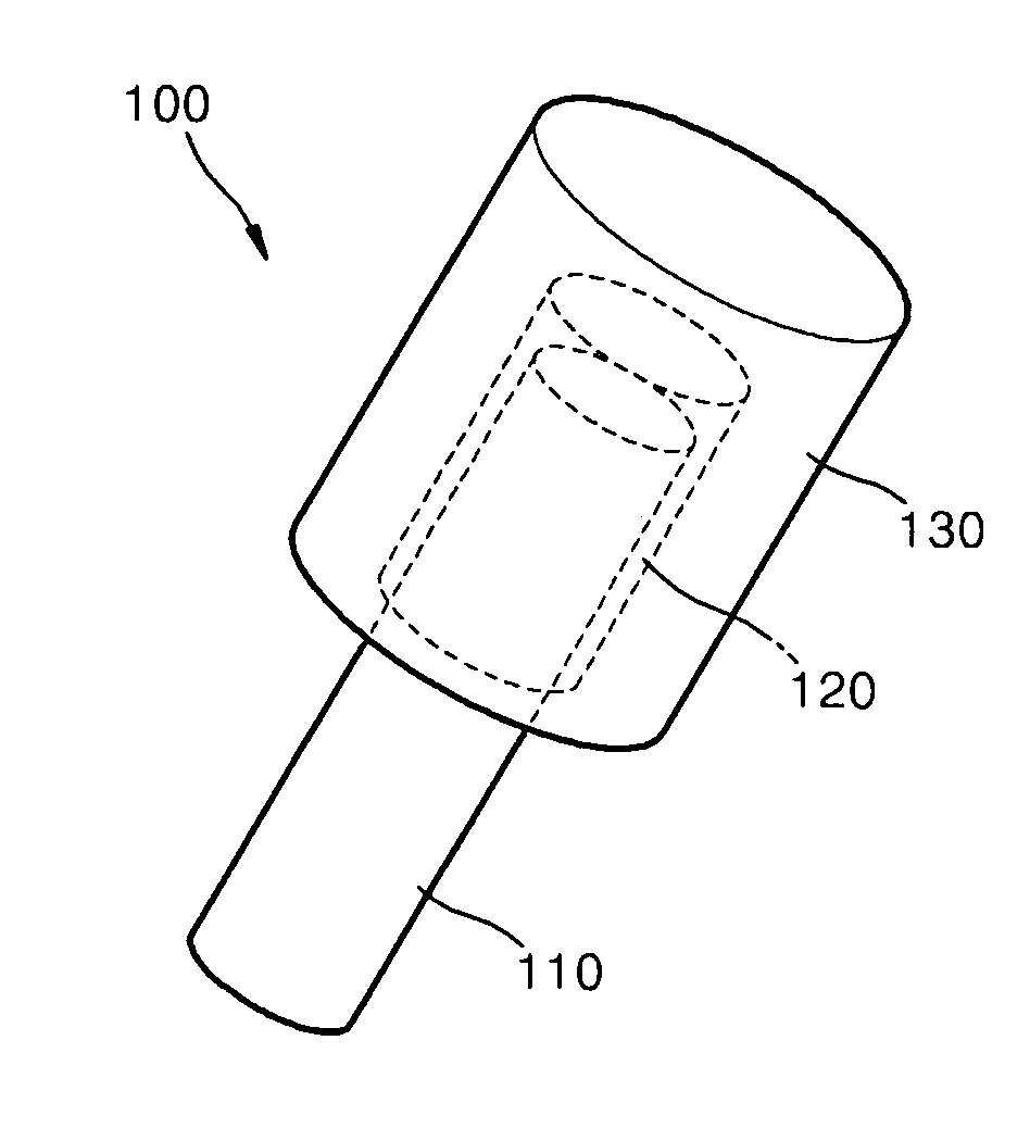
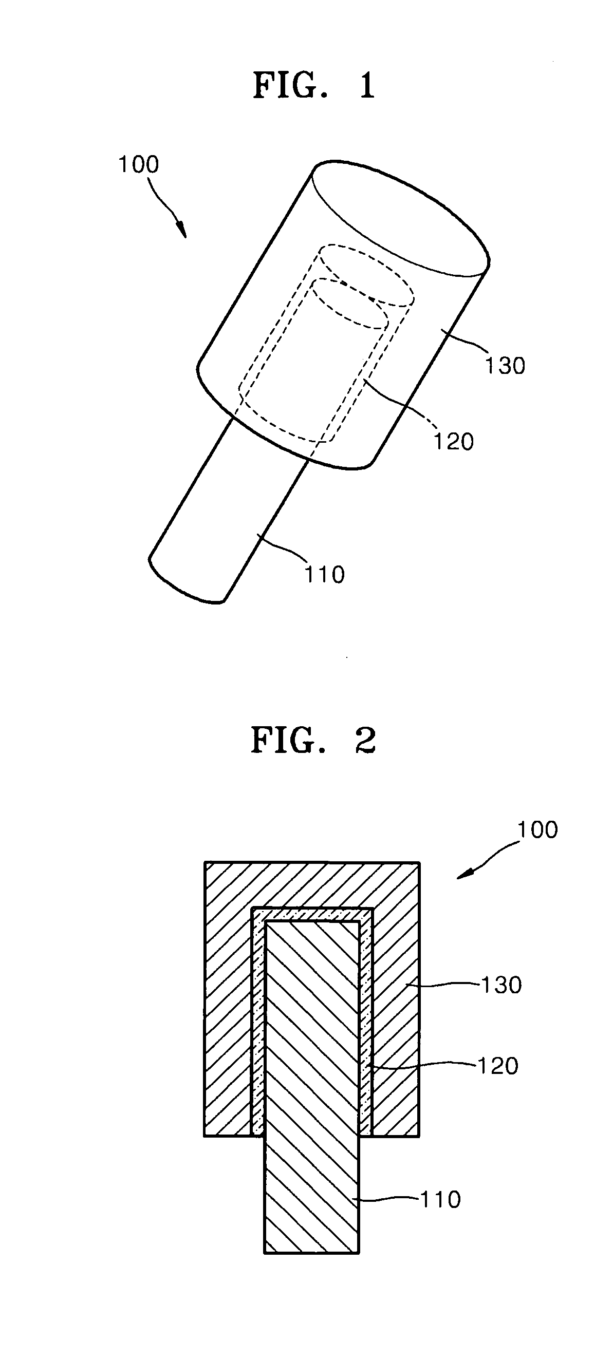
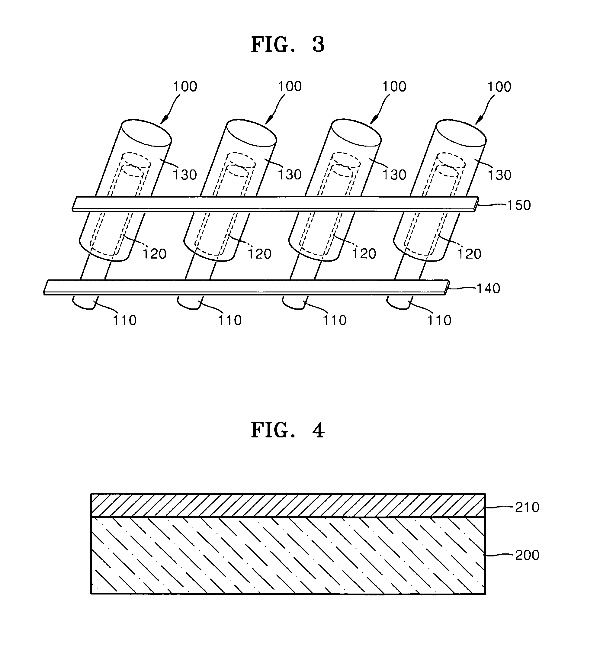
[0025]Various example embodiments will now be described more fully with reference to the accompanying drawings in which some example embodiments are shown. However, specific structural and functional details disclosed herein are merely representative for purposes of describing example embodiments. Thus, the invention may be embodied in many alternate forms and should not be construed as limited to only example embodiments set forth herein. Therefore, it should be understood that there is no intent to limit example embodiments to the particular forms disclosed, but on the contrary, example embodiments are to cover all modifications, equivalents, and alternatives falling within the scope of the invention.

[0026]Although the terms first, second, etc. may be used herein to describe various elements, these elements should not be limited by these terms. These terms are only used to distinguish one element from another. For example, a first element could be termed a second element, and, sim...


PUM


Abstract

A light emitting device using a micro-rod and a method of manufacturing a light emitting device are provided, the method includes forming a material layer on a substrate. The material layer is patterned such that a hole is formed that exposes a surface of the substrate. A core is grown in the shape of a micro-rod on the surface of the substrate exposed through the hole. A light emitting layer is deposited on the core. A shell is grown on the light emitting layer.

Description

CROSS-REFERENCE TO RELATED APPLICATIONS[0001]This application claims the benefit of priority under 35 U.S.C. §119 from Korean Patent Application No. 10-2008-0132512, filed on Dec. 23, 2008 in the Korean Intellectual Property Office, the disclosure of which is incorporated herein in its entirety by reference.BACKGROUND[0002]1. Field[0003]Example embodiments relate to a light emitting device using a micro-rod. Other example embodiments relate to a method of manufacturing a light emitting device.[0004]2. Description of the Related Art[0005]Research studies have been conducted on nanowires due to their electrical and optical characteristics, and applicability as a light emitting device. In particular, gallium nitride (GaN) nanowires have relatively minor defects that frequently occur in typical light emitting devices (e.g., light emitting diodes (LED) or laser diodes (LD)). For example, defects caused by lattice mismatch between a substrate and GaN are reduced. Research has been conduct...

Claims


Application Information

Patent Timeline
Patent Type & Authority Applications(United States)
IPC IPC(8): H01L33/00H01L21/00
CPCH01L21/02381H01L21/02458H01L21/0254H01L21/0259H01L33/18H01L21/02636H01L33/007H01L33/24H01L33/44H01L21/0262
Inventor LEE, MOON-SANGPARK, SUNG-SOO
Owner SAMSUNG ELECTRONICS CO LTD
Why Eureka
Try Eureka