Semiconductor device and driving method thereof
a technology of mikro-conductor and driving method, which is applied in the direction of digital storage, pulse automatic control, instruments, etc., can solve the problem that the extension of the clock transmission path may become a limitation in the design of the layou
- Summary
- Abstract
- Description
- Claims
- Application Information
AI Technical Summary
Benefits of technology
Problems solved by technology
Method used
Image

Examples
first embodiment
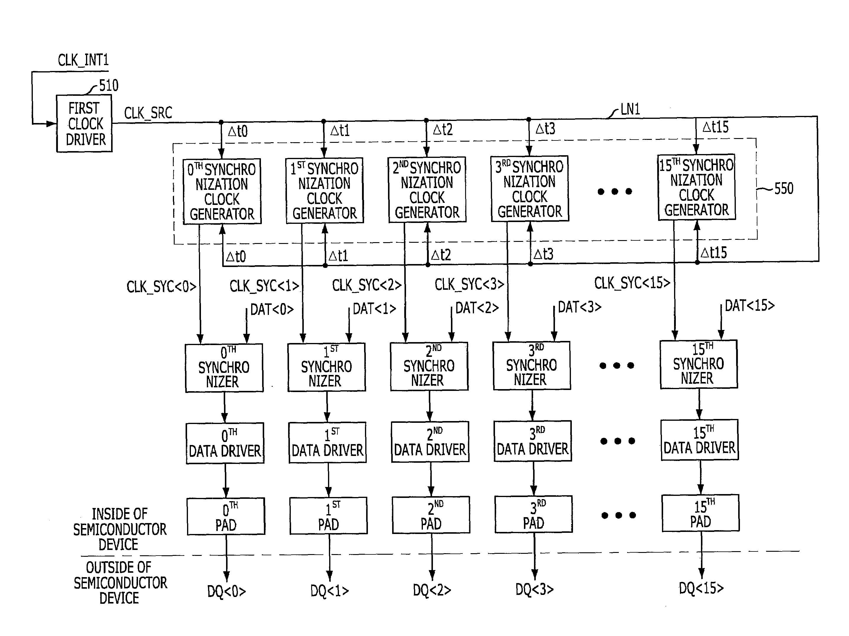
[0042]FIG. 5 is a block diagram illustrating a partial structure of a semiconductor device in accordance with the present invention.
[0043]Referring to FIG. 5, the semiconductor device according to the present embodiment includes a first clock driver 510, a second clock driver 530, a plurality of synchronization clock generators 550, a plurality of data output units 570, and a plurality of pads 590. The plurality of data output units 570 includes each of a plurality of synchronizers 572 and a plurality of data drivers 574.
[0044]For illustration purposes, FIG. 5 shows the semiconductor device including 16 pads 170, that is, 0th to 15th PAD as an example. Accordingly, the semiconductor device according to the present embodiment of FIG. 5 includes 16 synchronization clock generators 550 such as 0th to 15th SYNCHRONIZATION CLOCK GENERATOR, 16 synchronizers 572 such as 0th to 15th SYNCHRONIZER and 16 data drivers 574 such as 0th to 15th DATA DRIVER corresponding to the 16 pads.
[0045]The f...
second embodiment
[0081]FIG. 10 is a block diagram illustrating a partial structure of a semiconductor device in accordance with the present invention. For illustration purposes, like numeral references denote like elements in FIGS. 5 and 10. Compared to the semiconductor device of FIG. 5, the semiconductor device of FIG. 10 has a different clock transmission path for transferring a source clock signal.
[0082]Referring to FIG. 10, the semiconductor device according to the present embodiment inputs a source clock signal CLK_SRC to a plurality of synchronization clock generator 550 in a forward direction and in a backward direction through a clock transmission path LN1. That is, the semiconductor device of FIG. 10 may include one clock transmission path LN1 while the semiconductor device of FIG. 5 includes two clock transmission paths LN1 and LN2 (see FIG. 5).
[0083]Each of the plurality of synchronization clock generators 550, as shown in FIG. 6, includes a first input end and a second input end wherein...
third embodiment
[0086]FIG. 11 is a block diagram illustrating a partial structure of a semiconductor device in accordance with the present invention. For convenience, like numeral references denote like element in FIGS. 5 and 11. Compared to the semiconductor device of FIG. 5, the semiconductor device of FIG. 11 has a different clock transmission path and further includes a buffering unit 1110.
[0087]Referring to FIG. 11, the buffering unit 1110 outputs a second source clock signal CLK_SRC2 by buffering a first source clock signal CLK_SRC. Here, the buffering unit 1110 may be disposed on the second clock transmission path LN2 and the position thereof may differ according to design.
[0088]The semiconductor device according to the present embodiment may include a first clock transmission path LN1 for sequentially applying a first source clock signal CLK_SRC1 transferred in a forward direction to a plurality of synchronization clock generators 550 and a second clock transmission path LN2 for sequentiall...
PUM
 Abstract
Description
Claims
Application Information
 - R&D Engineer
- R&D Manager
- IP Professional
- Industry Leading Data Capabilities
- Powerful AI technology
- Patent DNA Extraction
Browse by: Latest US Patents, China's latest patents, Technical Efficacy Thesaurus, Application Domain, Technology Topic.
© 2024 PatSnap. All rights reserved.Legal|Privacy policy|Modern Slavery Act Transparency Statement|Sitemap