
Semiconductor device and driving method thereof

a technology of mikro-conductor and driving method, which is applied in the direction of digital storage, pulse automatic control, instruments, etc., can solve the problem that the extension of the clock transmission path may become a limitation in the design of the layou

Inactive Publication Date: 2011-10-11
SK HYNIX INC
View PDF13 Cites 3 Cited by
  • Summary
  • Abstract
  • Description
  • Claims
  • Application Information

AI Technical Summary

Benefits of technology

The present invention provides a semiconductor device that generates a synchronization clock signal using a total delay amount of a clock transmission path. The device also generates multiple synchronization clock signals that toggle at the same time using source clock signals that are delayed. The device eliminates a skew problem of the synchronization clock signals and maximizes the valid data range of the outputted data. The technical effects of the invention are improved synchronization and data output accuracy.

Problems solved by technology

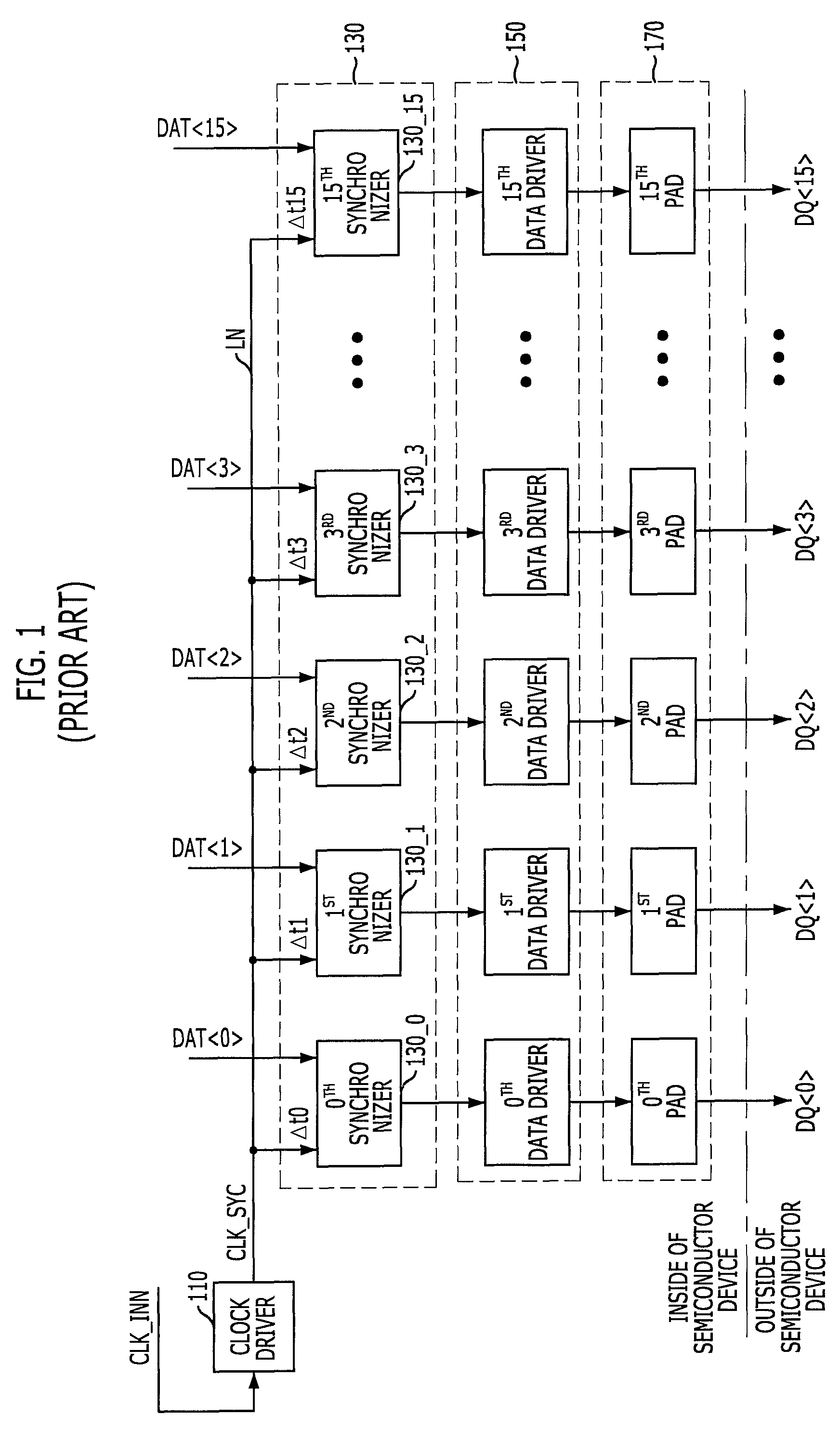
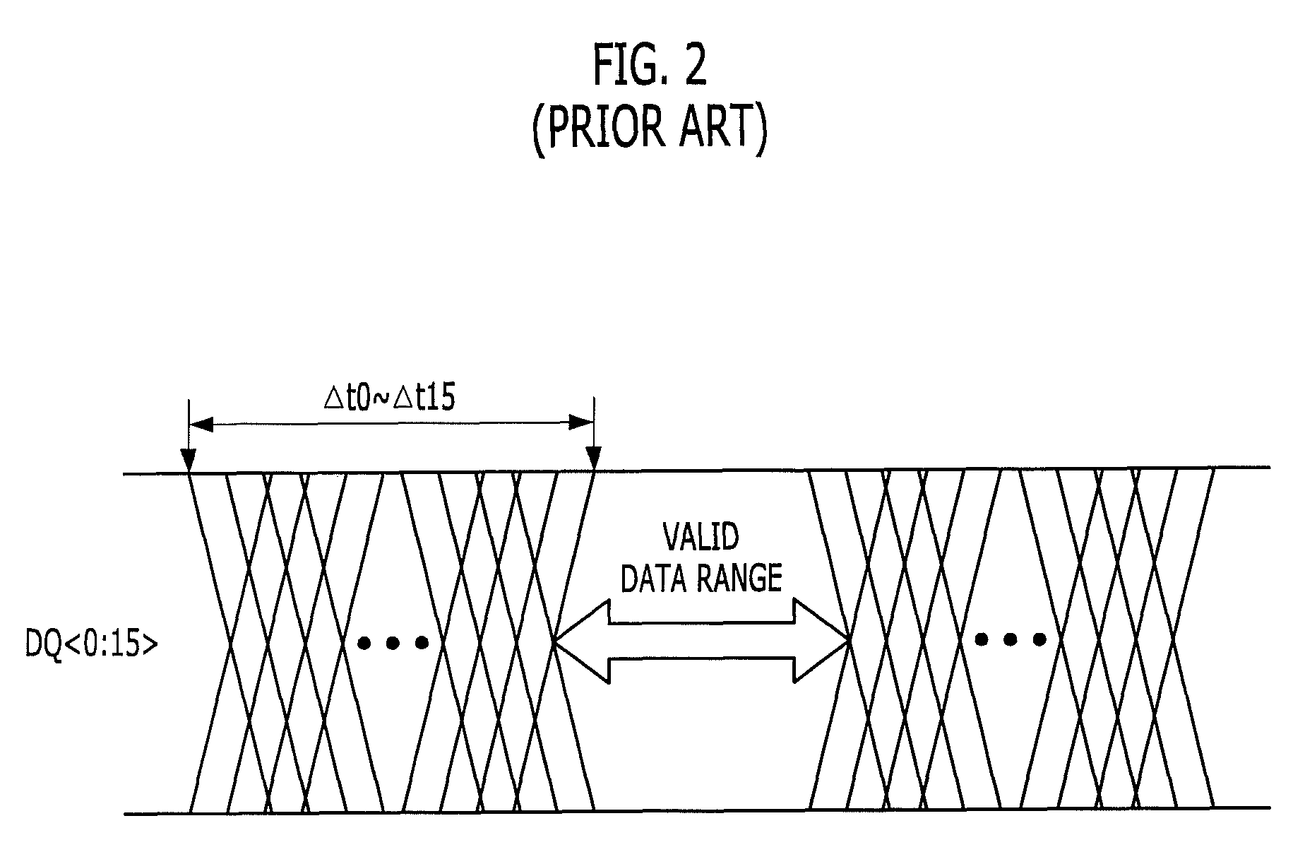
However, the semiconductor device of FIG. 3 has following problems.
However, such extension of the clock transmission path may become a limitation in designing a layout due to the high integration of the semiconductor device.

Method used


Image

  • Semiconductor device and driving method thereof
  • Semiconductor device and driving method thereof
  • Semiconductor device and driving method thereof

Examples


first embodiment

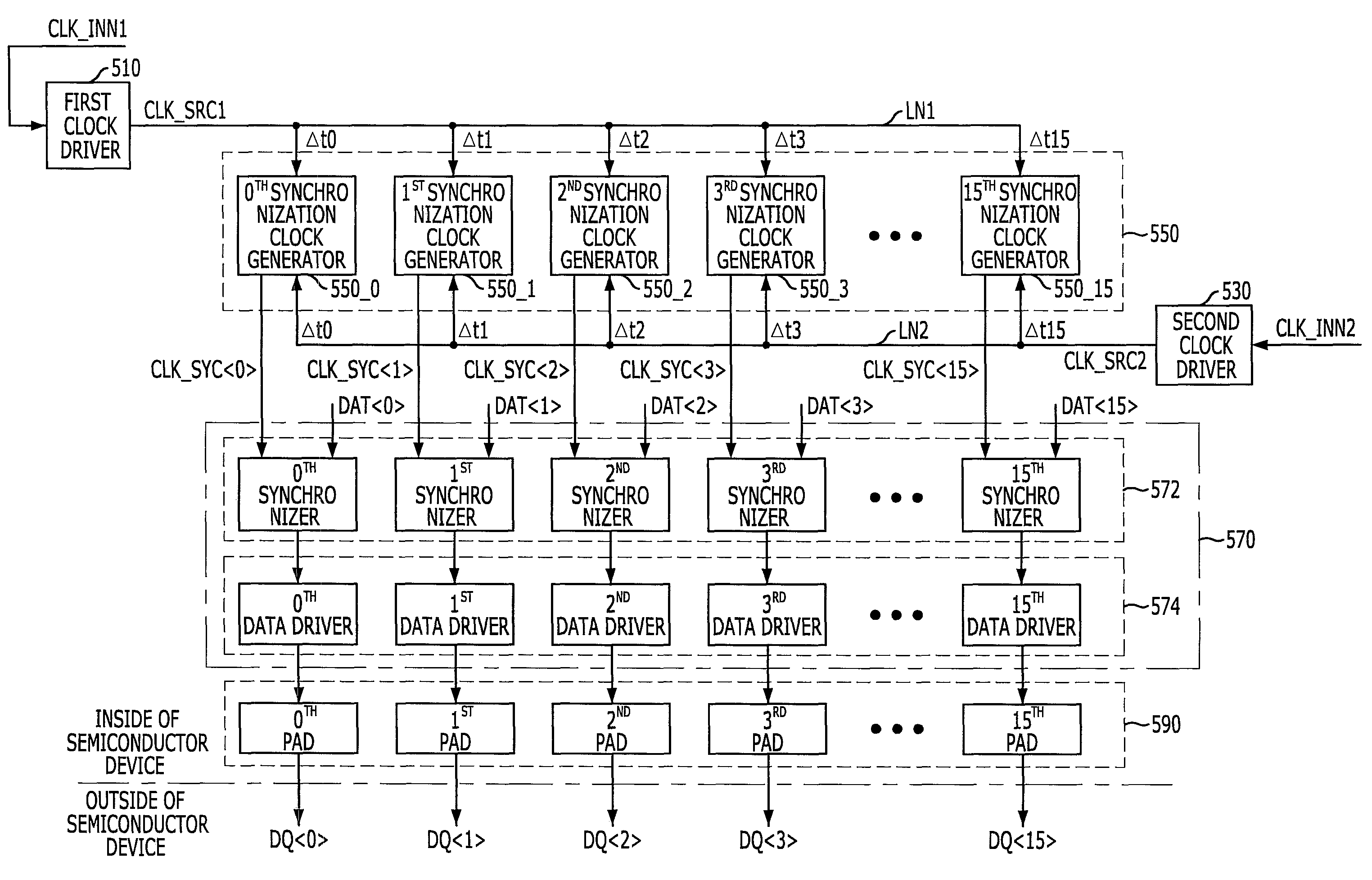
[0042]FIG. 5 is a block diagram illustrating a partial structure of a semiconductor device in accordance with the present invention.

[0043]Referring to FIG. 5, the semiconductor device according to the present embodiment includes a first clock driver 510, a second clock driver 530, a plurality of synchronization clock generators 550, a plurality of data output units 570, and a plurality of pads 590. The plurality of data output units 570 includes each of a plurality of synchronizers 572 and a plurality of data drivers 574.

[0044]For illustration purposes, FIG. 5 shows the semiconductor device including 16 pads 170, that is, 0th to 15th PAD as an example. Accordingly, the semiconductor device according to the present embodiment of FIG. 5 includes 16 synchronization clock generators 550 such as 0th to 15th SYNCHRONIZATION CLOCK GENERATOR, 16 synchronizers 572 such as 0th to 15th SYNCHRONIZER and 16 data drivers 574 such as 0th to 15th DATA DRIVER corresponding to the 16 pads.

[0045]The f...

second embodiment

[0081]FIG. 10 is a block diagram illustrating a partial structure of a semiconductor device in accordance with the present invention. For illustration purposes, like numeral references denote like elements in FIGS. 5 and 10. Compared to the semiconductor device of FIG. 5, the semiconductor device of FIG. 10 has a different clock transmission path for transferring a source clock signal.

[0082]Referring to FIG. 10, the semiconductor device according to the present embodiment inputs a source clock signal CLK_SRC to a plurality of synchronization clock generator 550 in a forward direction and in a backward direction through a clock transmission path LN1. That is, the semiconductor device of FIG. 10 may include one clock transmission path LN1 while the semiconductor device of FIG. 5 includes two clock transmission paths LN1 and LN2 (see FIG. 5).

[0083]Each of the plurality of synchronization clock generators 550, as shown in FIG. 6, includes a first input end and a second input end wherein...

third embodiment

[0086]FIG. 11 is a block diagram illustrating a partial structure of a semiconductor device in accordance with the present invention. For convenience, like numeral references denote like element in FIGS. 5 and 11. Compared to the semiconductor device of FIG. 5, the semiconductor device of FIG. 11 has a different clock transmission path and further includes a buffering unit 1110.

[0087]Referring to FIG. 11, the buffering unit 1110 outputs a second source clock signal CLK_SRC2 by buffering a first source clock signal CLK_SRC. Here, the buffering unit 1110 may be disposed on the second clock transmission path LN2 and the position thereof may differ according to design.

[0088]The semiconductor device according to the present embodiment may include a first clock transmission path LN1 for sequentially applying a first source clock signal CLK_SRC1 transferred in a forward direction to a plurality of synchronization clock generators 550 and a second clock transmission path LN2 for sequentiall...


PUM


Abstract

A semiconductor device includes a plurality of synchronization clock generators configured to generate a plurality of synchronization clock signals by mixing phases of first and second source clock signals having an identical frequency, a first clock transmission path configured to sequentially apply the first source clock signal to the plurality of synchronization clock generators by transferring the first source clock signal in a forward direction, a second clock transmission path configured to sequentially apply the second source clock signal to the plurality of synchronization clock generators by transferring the second source clock signal in a backward direction, and a plurality of data output units configured to synchronize a plurality of data with the plurality of synchronization clock signals and outputting the synchronized plurality of data.

Description

CROSS-REFERENCE TO RELATED APPLICATIONS[0001]The present invention claims priority of Korean patent application number 10-2008-0137057, filed on Dec. 30, 2008, the disclosure of which is incorporated herein by reference in its entirety.BACKGROUND OF THE INVENTION[0002]The present invention relates to a semiconductor design technology, and more particularly, to a semiconductor device for generating a synchronization clock signal and outputting a plurality of data in synchronization with the synchronization clock signal, and a driving method thereof.[0003]In general, a semiconductor memory device such as Double Data Rate Synchronous DRAM (DDR SDRAM) includes tens of millions of memory cells for storing data. Such a semiconductor memory device stores or outputs data according to a command from a central processing unit (CPU). For example, when a CPU requires a write operation, a semiconductor memory device stores data in a memory cell corresponding to an address inputted from the CPU. ...

Claims


Application Information

Patent Timeline
Patent Type & Authority Patents(United States)
IPC IPC(8): H03L7/00
CPCG11C7/1051G11C7/1066G11C7/22G11C7/222H03L7/00G11C7/00G11C7/10G11C11/4063G11C11/4076
Inventor KIM, TAE-KYUN
Owner SK HYNIX INC
Learn More