Light-emitting device package structure and manufacturing method thereof

a technology of light-emitting devices and manufacturing methods, which is applied in the manufacturing of semiconductor/solid-state devices, semiconductor devices, electrical devices, etc., can solve the problem of limited viewing distance between the viewer and the christmas tr

Inactive Publication Date: 2010-07-29
EVERLIGHT ELECTRONICS
View PDF11 Cites 0 Cited by
  • Summary
  • Abstract
  • Description
  • Claims
  • Application Information

AI Technical Summary

Benefits of technology

[0008]It is therefore an objective of the present invention to provide a light-emitting device package structure and a manufacturing method thereof so as to increase the viewing distance of the Christmas lamp.
[0011]The present invention forms the gas space inside the light-emitting device package structure in the encapsulation process by the concavity of the light-emitting device structure. Therefore, the light emitted from the light-emitting device can be partially reflected by the gas space, and the light passing through the gas space can be condensed by the second encapsulated portion. Therefore, not only the luminous intensity of at the center of the optical axis of the light-emitting device package structure can be increased, but the light-emitting device package structure can also have sufficient luminous intensity at the edge.

Problems solved by technology

Therefore, when the light-emitting device package structure according to the prior art is applied to the Christmas tree, the viewing distance between the viewer and the Christmas tree is limited because of the limit of the luminous intensity of the light-emitting device package structure.

Method used


Image

  • Light-emitting device package structure and manufacturing method thereof
  • Light-emitting device package structure and manufacturing method thereof
  • Light-emitting device package structure and manufacturing method thereof

Examples


Embodiment Construction

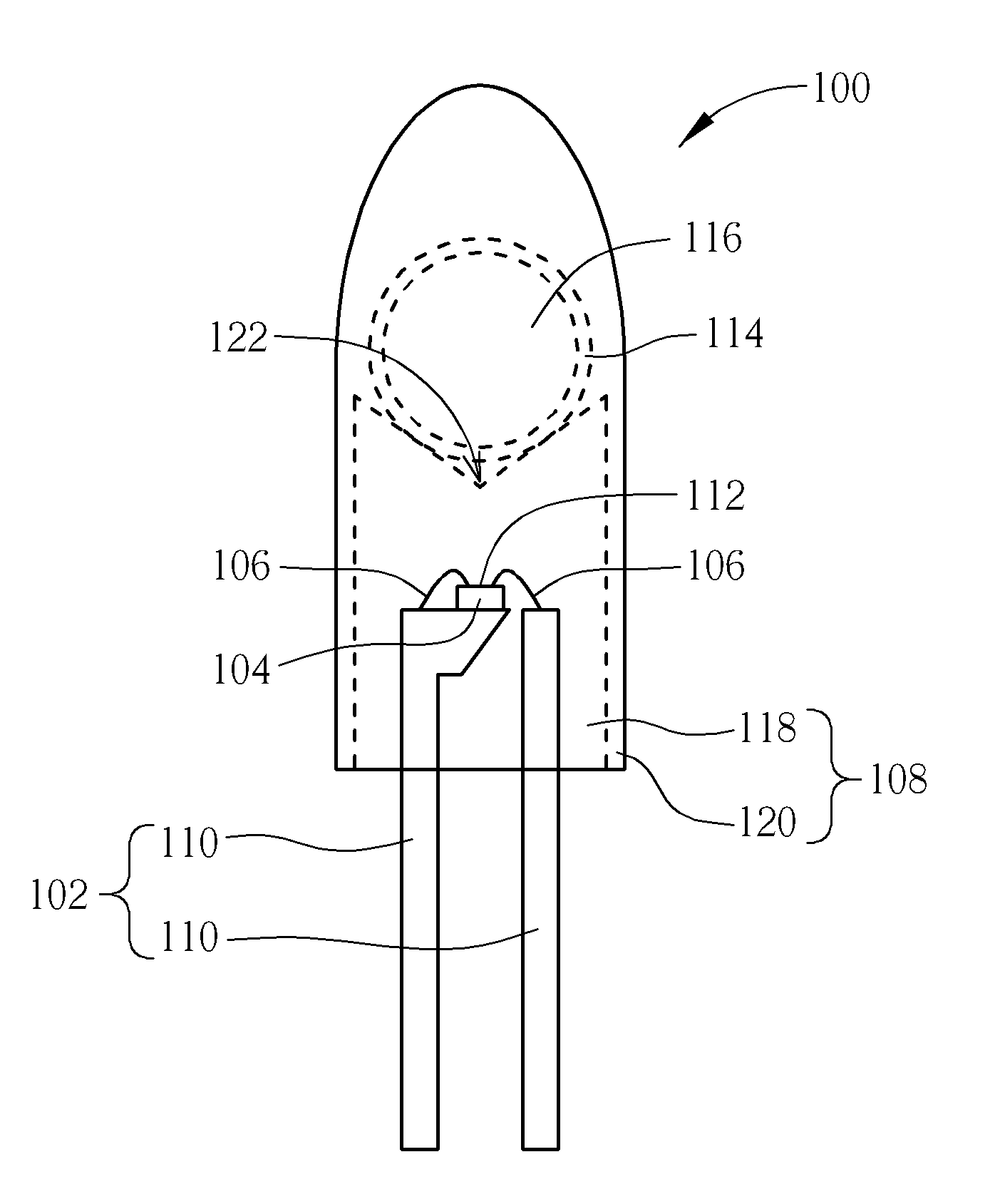
[0021]Referring to FIG. 3, FIG. 3 is a cross-sectional schematic diagram illustrating a light-emitting device package structure according to a first embodiment of the present invention. As shown in FIG. 3, the light-emitting device package structure 100 includes a leadframe 102, a light-emitting device 104, a plurality of wires 106, and an encapsulant 108. The leadframe 102 of this embodiment includes two leads 110, but the leadframe of the present invention is not limited to only have two leads. The number of leads can be increased according to the actual requirements. The light-emitting device 104 is disposed on one of the leads 110, and a top surface of the light-emitting device 104 is a main luminous surface. In addition, the light-emitting device 104 can be any kind of luminous device, such as a light emitting diode (LED) chip, LED device or organic LED device, etc. This embodiment takes the LED chip as an example, but this is not meant to be a limitation. Furthermore, each wir...


PUM


Abstract

A light-emitting device package structure includes a leadframe, a light-emitting device disposed on the leadframe, a plurality of wires electrically connecting the leadframe and the light-emitting device, and an encapsulant covering the light-emitting device, the wires and a part of the leadframe. The encapsulant has a gas space therein, and the gas space is disposed on the light-emitting device, wherein the gas space includes at least one gas.

Description

BACKGROUND OF THE INVENTION[0001]1. Field of the Invention[0002]The present invention relates to a light-emitting device package structure and a manufacturing method thereof, and more particularly, to a light-emitting device package structure with gas space and a manufacturing method thereof.[0003]2. Description of the Prior Art[0004]Conventional fairy lights that decorate Christmas trees are composed of many light bulbs, and require being uniformly disposed on the Christmas trees so as to exhibit the appearance of the Christmas trees at night. However, with the development of package technology, LEDs that have the advantages of small size, high shock resistance, low power consumption, long lifetime, no warm up time and fast response time have gradually replaced the conventional light bulbs.[0005]Referring to FIG. 1, FIG. 1 is a cross-sectional schematic diagram illustrating a light-emitting device package structure applied to Christmas trees according to the prior art. As shown in ...

Claims


Application Information

Patent Timeline
Patent Type & Authority Applications(United States)
IPC IPC(8): H01L33/52H01L33/62
CPCH01L33/52H01L33/56H01L2224/48091H01L2224/48247H01L2224/48257H01L2924/00014
Inventor CHEN, YING-ZHONGHSU, CHIH-HUNGHSU, CHIA-YUN
Owner EVERLIGHT ELECTRONICS
Why Eureka
Try Eureka