Silicon Substrate Having Through Vias and Package Having the Same

a technology of silicon substrate and through via, which is applied in the direction of semiconductor devices, electrical equipment, semiconductor/solid-state device details, etc., can solve the problems of poor heat dissipation efficiency of conventional substrates with through vias b>1/b>, and achieve noise isolation, good heat dissipation efficiency, and avoidance of signal interference

Active Publication Date: 2010-07-29
ADVANCED SEMICON ENG INC
View PDF13 Cites 31 Cited by
  • Summary
  • Abstract
  • Description
  • Claims
  • Application Information

AI Technical Summary

Benefits of technology

[0009]In this way, the heat in the through vias is transmitted to the heat dissipating area, and since the area of the heat dissipating area is large, the silicon substrate has good heat dissipation efficiency. Moreover, as the through vias inside the heat dissipating area have same electrical potential, the noise is isolated and signal interference can be avoided.

Problems solved by technology

The disadvantage of the conventional substrate having through vias 1 is as follows.
However, as the through vias 12 are filled with the conductive material 121, only little of the conductive material 121 is exposed to the surface 111 of the substrate 1, so the substrate 1 has poor heat dissipation efficiency.

Method used


Image

  • Silicon Substrate Having Through Vias and Package Having the Same
  • Silicon Substrate Having Through Vias and Package Having the Same
  • Silicon Substrate Having Through Vias and Package Having the Same

Examples


first embodiment

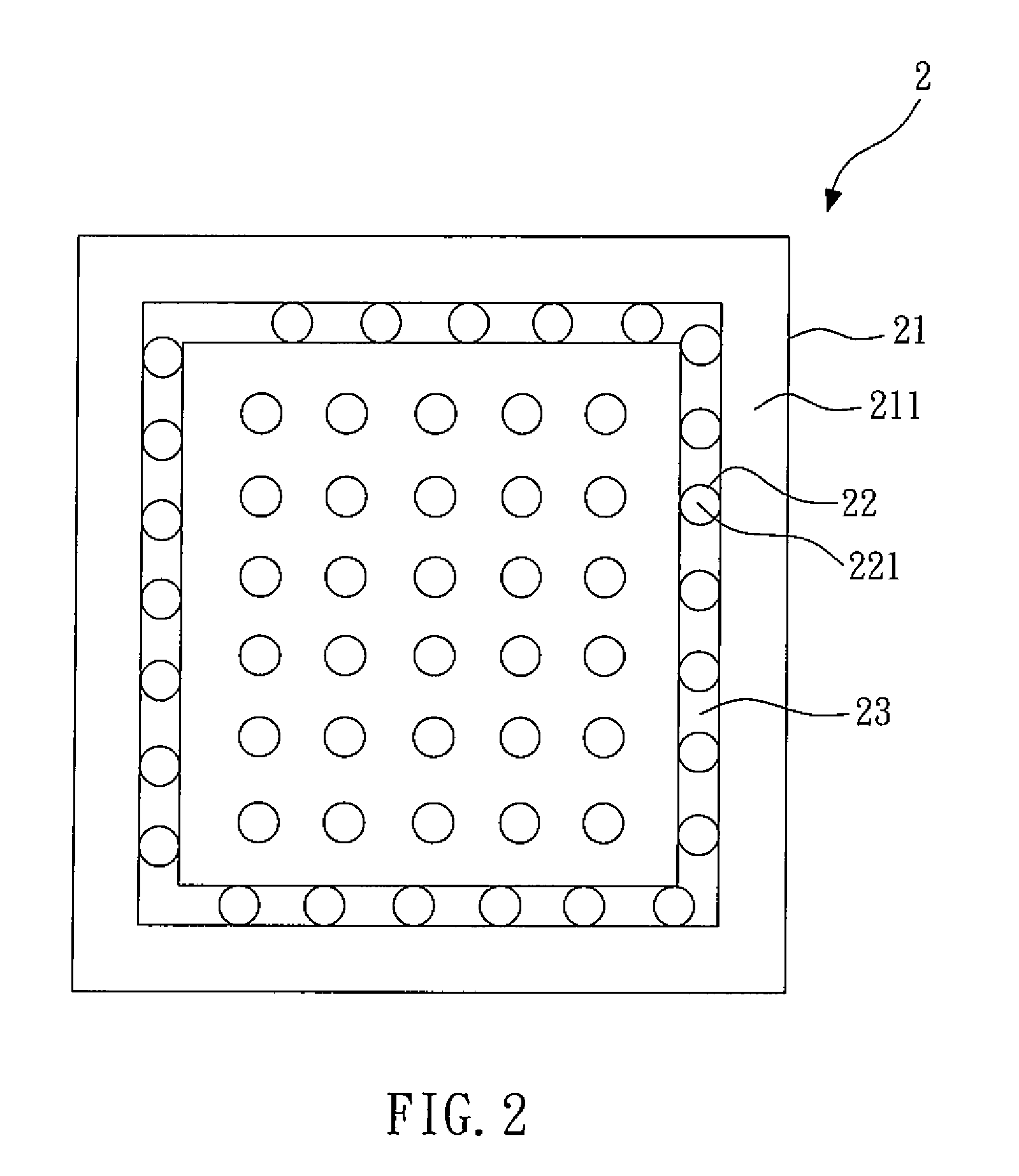
[0018]FIG. 2 shows a top view of a silicon substrate having through vias according to the present invention. The silicon substrate 2 comprises a substrate body 21, a plurality of through vias 22 and at least one heat dissipating area 23. The substrate body 21 has a surface 211, and the material of the substrate body 21 is silicon. The through vias 22 penetrate the substrate body 21, and each of the through vias 22 has a conductive material 221 therein. In the embodiment, the through vias 22 are filled with the conductive material 221. However, in other applications, the conductive material 221 may be electroplated on the inner wall of the through vias 22.

[0019]The heat dissipating area 23 is disposed on the surface 211 of the substrate body 21 and covers at least two through vias 22. The through vias 22 inside the heat dissipating area 23 have same electrical potential. The heat dissipating area 23 is made of metal, and the material of the heat dissipating area 23 is preferably copp...

second embodiment

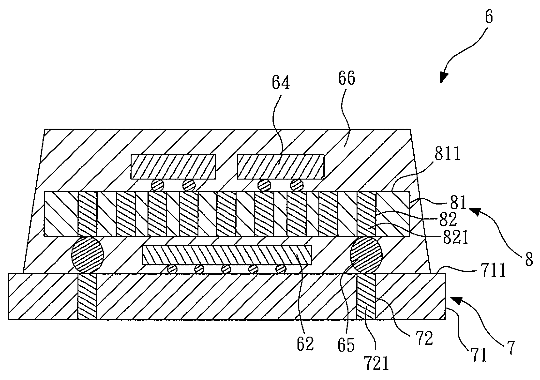
[0032]In the embodiment, the second substrate 8 is the same as the silicon substrate 3 (FIG. 3) according to the However, it is understood that the second substrate 8 may be the silicon substrates shown in FIG. 2, FIG. 4 or FIG. 5.

[0033]As shown in FIG. 6, the second chip 64 is disposed on the second substrate8, and electrically connected to the second substrate 8. The connecting elements 65, e.g. solder balls, electrically connect the second through vias 82 of the second substrate 8 to the first substrate 7. In the embodiment, the molding compound 66 encapsulates the first substrate 7, the first chip 62, the second substrate 8, the second chip 64 and the connecting elements 65.


PUM

PropertyMeasurementUnit
conductiveaaaaaaaaaa
electrical potentialaaaaaaaaaa
heat dissipating areaaaaaaaaaaa

Abstract

The present invention relates to a silicon substrate having through vias and a package having the same. The silicon substrate includes a substrate body, a plurality of through vias and at least one heat dissipating area. The substrate body has a surface, and the material of the substrate body is silicon. The through vias penetrate the substrate body, and each of the through vias has a conductive material therein. The heat dissipating area is disposed on the surface of the substrate body and covers at least two through vias. The heat dissipating area is made of metal, and the through vias inside the heat dissipating area have same electrical potential. Thus, the heat in the through vias is transmitted to the heat dissipating area, and since the area of the heat dissipating area is large, the silicon substrate has good heat dissipation efficiency.

Description

BACKGROUND OF THE INVENTION[0001]1. Field of the Invention[0002]The present invention relates to a silicon substrate and a package having the same, and more particularly to a silicon substrate having through vias and a package having the same.[0003]2. Description of the Related Art[0004]FIG. 1 shows a top view of a conventional substrate having through vias. The substrate 1 comprises a substrate body 11 and a plurality of through vias 12. The substrate body 11 has a surface 111. The through vias 12 penetrate the substrate body 11, and each of the through vias 12 has a conductive material 121 therein. The through vias 12 are filled with the conductive material 121.[0005]The disadvantage of the conventional substrate having through vias 1 is as follows. The material of the conductive material 121 of the through vias 12 of the substrate 1 is usually metal, because metal is good heat conductor. However, as the through vias 12 are filled with the conductive material 121, only little of t...

Claims


Application Information

Patent Timeline
Patent Type & Authority Applications(United States)
IPC IPC(8): H01L23/34H01L23/48
CPCH01L23/147H01L23/3677H01L23/49816H01L23/49827H01L24/16H01L25/0652H01L2224/16235H01L2225/06517H01L2225/0652H01L2225/06572H01L2225/06589H01L2924/15311H01L2224/16H01L2224/16225H01L2924/00011H01L2924/00014H01L2224/0401
Inventor CHEN, KUO-HUAYANG, KUO-PIN
Owner ADVANCED SEMICON ENG INC
Why Eureka
Try Eureka