

Semiconductor device and method of manufacturing the same, and electronic apparatus
a semiconductor device and semiconductor technology, applied in the direction of semiconductor devices, semiconductor/solid-state device details, electrical apparatus, etc., can solve the problems of increasing the size in the height direction of the semiconductor device b>201/b> and the size in the thickness direction of the electronic apparatus b>200/b>, so as to reduce the size
- Summary
- Abstract
- Description
- Claims
- Application Information
AI Technical Summary
Benefits of technology
Problems solved by technology
Method used
Image

Examples
first embodiment
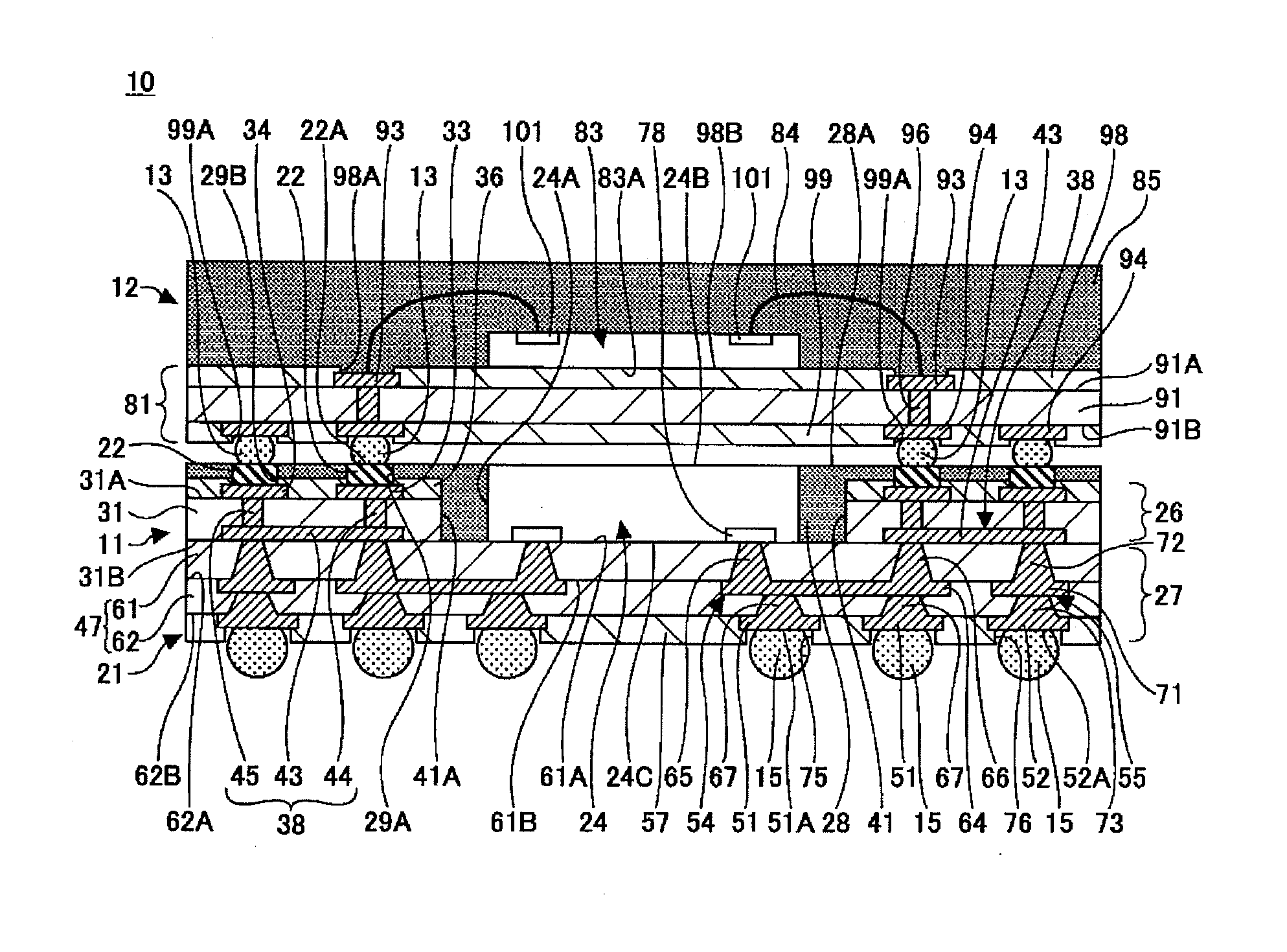
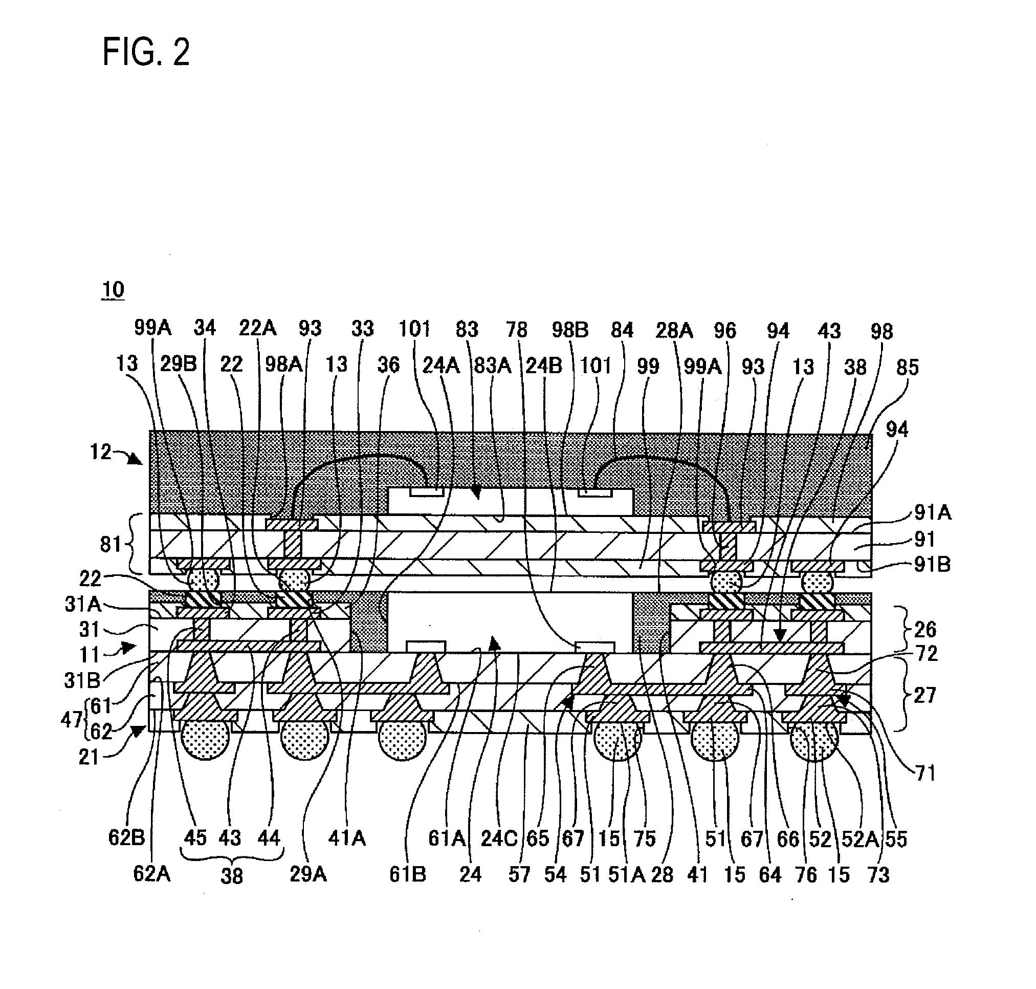
[0055]FIG. 2 is a sectional view showing an electronic apparatus according to a first embodiment of the invention.
[0056]With reference to FIG. 2, an electronic apparatus 10 according to the first embodiment has a semiconductor device 11, a semiconductor device 12 to be another semiconductor device, an internal connecting terminal 13 and an external connecting terminal 15.
[0057]The semiconductor device 11 has a wiring board 21, a conductive member 22 and an electronic component 24. The wiring board 21 has a first multilayer wiring structure 26, a second multilayer wiring structure 27, a sealing resin 28 and opening portions 29A and 29B.
[0058]The first multilayer wiring structure 26 is disposed on the second multilayer wiring structure 27 to be opposed to a side surface 24A of the electronic component 24. The first multilayer wiring structure 26 is caused to take such a shape as to surround the side surface 24A of the electronic component 24 (more specifically, a shape of a frame seen...
second embodiment
[0133]FIG. 16 is a sectional view showing an electronic apparatus according to a second embodiment of the invention. In FIG. 16, the same components as those of the electronic apparatus 10 according to the first embodiment have the same designations.
[0134]With reference to FIG. 16, an electronic apparatus 110 according to the second embodiment has the same structure as that of the electronic apparatus 10 except that a semiconductor device 111 and an internal connecting terminal 113 are provided in place of the semiconductor device 11 and the internal connecting terminal 13 which are provided in the electronic apparatus 10 according to the first embodiment, and a resin member 115 is further provided.
[0135]The semiconductor device 111 has the same structure as that of the semiconductor device 10 except that the conductive member 22 provided in the semiconductor device 10 described in the first embodiment is excluded from the components.
[0136]The semiconductor device 111 according to t...
PUM
 Abstract
Description
Claims
Application Information