Semiconductor integrated circuit

Inactive Publication Date: 2010-08-19
RENESAS ELECTRONICS CORP
View PDF4 Cites 1 Cited by
  • Summary
  • Abstract
  • Description
  • Claims
  • Application Information

AI Technical Summary

Benefits of technology

[0010]As is obvious from the above description, there is a strong demand for conducting a delay test under actual operating conditions for a semiconductor integrated circuit including multiple logic circuits that operate based on clocks of different frequencies, without causing any inconveniences when the test clock is set to one of the high-frequency side and the low-frequency side.
[0012]In the semiconductor integrated circuit according to the first exemplary aspect of the present invention, the test circuit is first connected between the first and second logic circuits. During a delay test for the first logic circuit, the test circuit outputs the output of the first logic circuit without passing through the second logic circuit. Further, during a test for the second logic circuit, the test circuit transmits the input value received without being passed through the first logic circuit, to the second logic circuit. Furthermore, during the tests for the logic circuits, the test circuit carries out different operations between the tests. This makes it possible to conduct delay tests under actual operating conditions without causing any inconveniences when the test clock is set to one of the high-frequency side and the low-frequency side.
[0014]According to exemplary aspects of the present invention, it is possible to conduct delay tests under actual operating conditions for a semiconductor integrated circuit including multiple logic circuits that operate based on clocks of different frequencies, without causing any inconveniencies when a test clock is set to one of a high-frequency side and a low-frequency side.

Problems solved by technology

It is impractical in many aspects (e.g., an increase in circuit area due to an additional circuit) to design and produce the circuit block, which operates based on the low frequency clock, so as to be able to operate based also on the high frequency clock for the test.
Note that when the test clock is set to the low frequency clock, it is impossible to detect a delay which occurs during actual operation of the circuit block that operates based on the high frequency clock, and it is impossible to increase the level of the delay test in the first place.

Method used


Image

  • Semiconductor integrated circuit
  • Semiconductor integrated circuit
  • Semiconductor integrated circuit

Examples


first exemplary embodiment

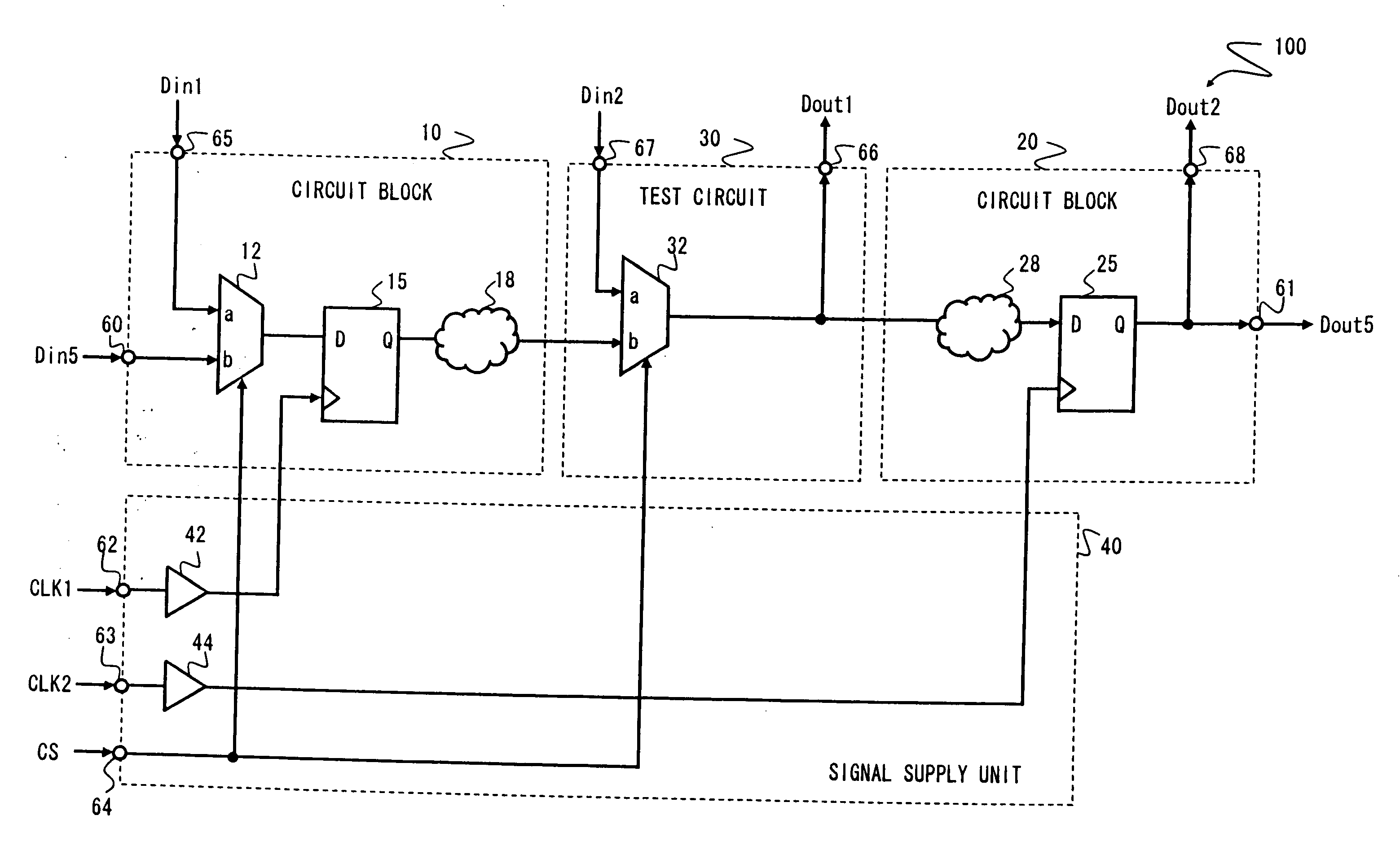
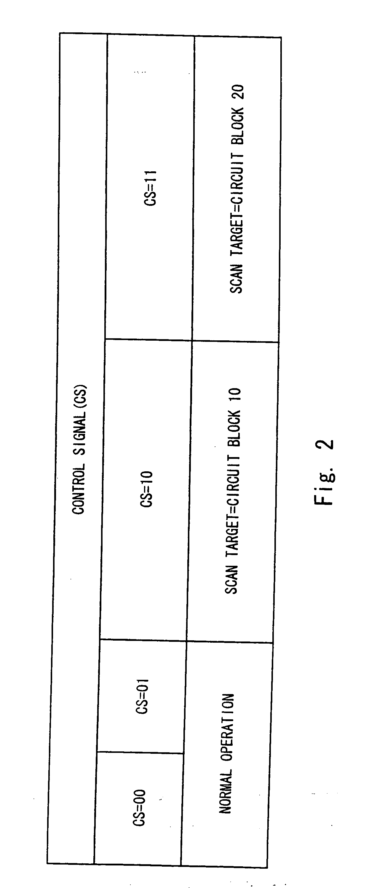
[0029]A first exemplary embodiment of the present invention will be described below with reference to FIGS. 1 to 6. FIG. 1 is a schematic circuit diagram of a semiconductor integrated circuit according to the first exemplary embodiment. FIG. 2 is an exemplary diagram illustrating control operation for the semiconductor integrated circuit based on a control signal. FIG. 3 is an explanatory diagram illustrating operating states and operating conditions of the semiconductor integrated circuit at the time of scanning. FIGS. 4 to 6 are schematic timing diagrams each illustrating the operation of the semiconductor integrated circuit at the time of scanning.

[0030]As shown in FIG. 1, a semiconductor integrated circuit 100 includes a circuit block 10, a circuit block 20, a test circuit 30, and a signal supply circuit 40. The circuit block 10 includes a selector 12, a F / F 15, and a net 18. The circuit block 20 includes a net 28 and a F / F 25. The test circuit 30 includes a selector 32 and a la...

second exemplary embodiment

[0068]Referring to FIGS. 8 to 11, a second exemplary embodiment of the present invention will be described. FIG. 8 is a schematic circuit diagram of a semiconductor integrated circuit according to the second exemplary embodiment. FIGS. 9 to 11 are schematic timing diagrams each illustrating the operation of the semiconductor integrated circuit at the time of scanning.

[0069]As shown in FIG. 8, unlike the first exemplary embodiment, the test circuit 30 according to this exemplary embodiment does not include the latch 35, and the signal supply circuit 40 does not include the selector 45. Also in this case, as in the first exemplary embodiment, it is possible to conduct the delay tests for the circuit blocks 10 and 20 independently by using clocks of actual operating frequencies. This makes it possible to effectively avoid the occurrence of inconveniences caused by setting the test clock to the high frequency clock or the low frequency clock as in the conventional case.

[0070]According t...


PUM


Abstract

An exemplary aspect of the invention is to conduct delay tests under actual operating conditions for a semiconductor integrated circuit including multiple logic circuits operating based on clocks of different frequencies, without causing any inconveniences when a test clock is set to a high-frequency side or a low-frequency side. The semiconductor integrated circuit includes: a first logic block that operates based on a first clock; a second logic block that operates based on a second clock having a frequency different from that of the first clock; and a test circuit connected between the first logic block and the second logic block. The test circuit outputs an output of the first logic block set as a test target, without passing through the second logic block, and transmits an input value received without being passed through the first logic circuit, to the second logic circuit set as a test target.

Description

INCORPORATION BY REFERENCE[0001]This application is based upon and claims the benefit of priority from Japanese patent application No. 2009-032898, filed on Feb. 16, 2009, the disclosure of which is incorporated herein in its entirety by reference.BACKGROUND[0002]1. Field of the Invention[0003]The present invention relates to a semiconductor integrated circuit, and more particularly, to a semiconductor integrated circuit including a test circuit.[0004]2. Description of Related Art[0005]With the recent remarkable development of technology for semiconductor integrated circuits, multiple circuit blocks that operate based on clocks of different frequencies may be incorporated into a single circuit chip. In such a case, both a logic test and a delay test are usually carried out to secure the reliability of the circuit chip.[0006]Japanese Unexamined Patent Application Publication No. 56-168268 discloses a technique for diagnosing asynchronous operation by use of a scan-in / scan-out techniq...

Claims


Application Information

Patent Timeline
IPC IPC(8): H03K19/00
CPCG01R31/31858G01R31/31725
Inventor YAMAMOTO, MITSUHIRO
Owner RENESAS ELECTRONICS CORP
Why Eureka
Try Eureka