Dividing pixels between chiplets in display device

a display device and chiplet technology, applied in semiconductor devices, digital transmission, instruments, etc., can solve the problems of non-uniform electrical performance and visual appearance of display devices employing such materials, affecting the image quality of display, and large thin film transistors (tfts) made from amorphous or polycrystalline silicon are relatively large, so as to improve color mixing and pixel uniformity

Active Publication Date: 2010-08-19
GLOBAL OLED TECH
View PDF8 Cites 108 Cited by
  • Summary
  • Abstract
  • Description
  • Claims
  • Application Information

AI Technical Summary

Benefits of technology

[0015]The present invention has the advantage that, by providing pixels having sub-pixels controlled by more than one chiplet, improved color mixing and pixel uniformity is achieved.

Problems solved by technology

Thin-film transistors (TFTs) made from amorphous or polycrystalline silicon are relatively large and have lower performance compared to conventional transistors made in crystalline silicon wafers.
Moreover, such thin-film devices typically exhibit local or large-area non-uniformity across the glass substrate that results in non-uniformity in the electrical performance and visual appearance of displays employing such materials.
The larger chiplets can detrimentally affect the image quality of the display.

Method used


Image

  • Dividing pixels between chiplets in display device
  • Dividing pixels between chiplets in display device
  • Dividing pixels between chiplets in display device

Examples


Embodiment Construction

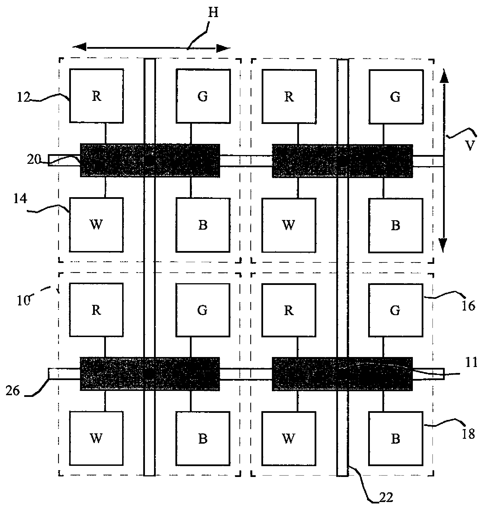
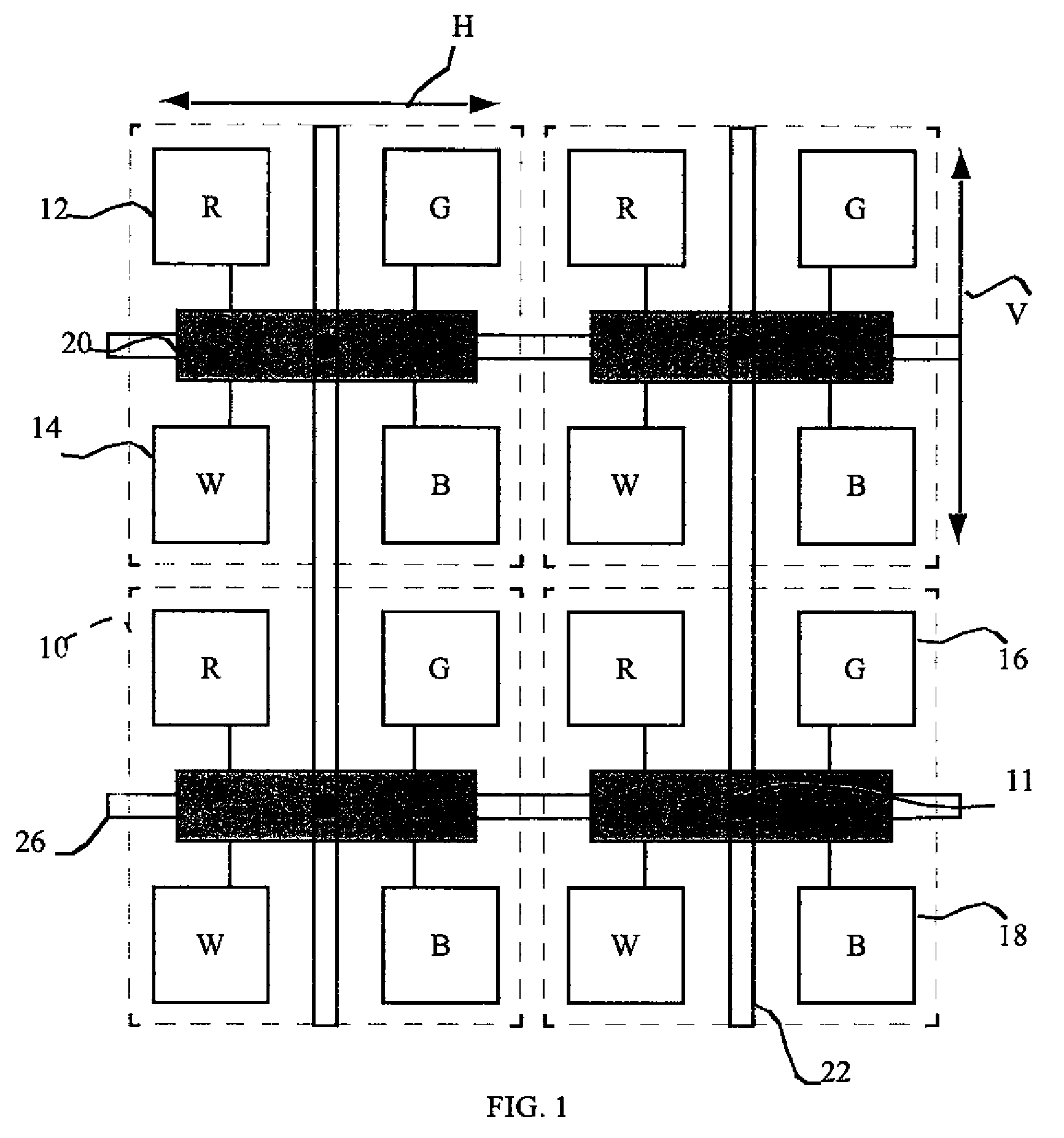
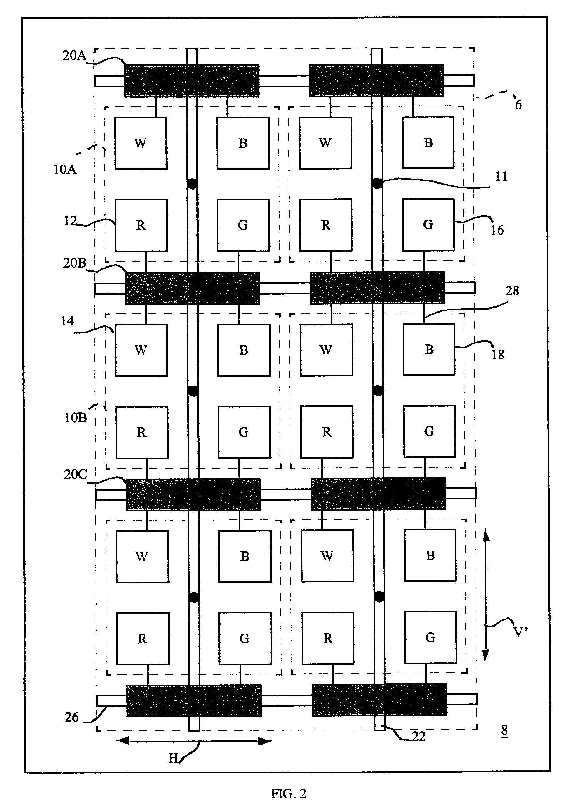
[0032]Conventional active-matrix displays employ thin-film transistor circuits comprising amorphous or polysilicon films deposited on a substrate to control the display elements. These thin-film transistors, however, have much lower performance than the crystalline silicon devices typically used in integrated circuits. An alternative control method for active-matrix devices employs a plurality of chiplets located over a substrate in the light-emitting area of a display. Each chiplet is formed on a substrate independent of the display substrate and includes circuitry and connection pads for driving the electrodes of the light-emitting or light-controlling elements in the display and for responding to signals from a controller external to the display.

[0033]Referring to FIG. 1, a partial schematic of a display device illustrates a plurality of pixels 10 including four sub-pixels defining a light-emitting display area. The display device further includes a plurality of chiplets 20 locat...


PUM


Abstract

A display device includes a substrate, a plurality of pixels formed over the substrate, each pixel including two or more sub-pixels, the plurality of pixels defining a display area, and a plurality of chiplets located over the substrate in the display area, each chiplet controlling sub-pixels of at least two adjacent pixels.

Description

FIELD OF THE INVENTION[0001]The present invention relates to display devices having a substrate with distributed, independent chiplets for controlling a pixel array and, more particularly, to the control of sub-pixels in for each pixel in the array.BACKGROUND OF THE INVENTION[0002]Flat-panel display devices are widely used in conjunction with computing devices, in portable devices, and for entertainment devices such as televisions. Such displays typically employ a plurality of pixels distributed over a substrate to display images. Each pixel incorporates several, differently colored light-emitting elements commonly referred to as sub-pixels, typically emitting red, green, and blue light, to represent each image element or pixel. A variety of flat-panel display technologies are known, for example plasma displays, liquid crystal displays, and light-emitting diode (LED) displays.[0003]Light emitting diodes (LEDs) incorporating thin films of light-emitting materials forming light-emitti...

Claims


Application Information

Patent Timeline
Patent Type & Authority Applications(United States)
IPC IPC(8): G09G3/32
CPCG09G3/20G09G3/2088G09G3/3208G09G2300/0426H01L27/3255G09G2320/0233G09G2320/0242H01L27/3213G09G2300/0452H10K59/351H10K59/129G09G3/32H04L27/00
Inventor COK, RONALD S.
Owner GLOBAL OLED TECH
Why Eureka
Try Eureka