Integrated circuit structure and a method of forming the same

a technology of integrated circuits and components, applied in the direction of radiating element structural forms, antennas, electrical devices, etc., can solve the problems of reducing transmission loss, difficult to achieve wide impedance matching bandwidth using inductive feeding, and extremely difficult to realize bond wire feeding at 60 ghz in mmw aip designs

Inactive Publication Date: 2010-09-02
NANYANG TECH UNIV
View PDF9 Cites 51 Cited by
  • Summary
  • Abstract
  • Description
  • Claims
  • Application Information

AI Technical Summary

Problems solved by technology

The wire line is necessary because the multi-chip module solution of the Tx or Rx does not allow for the Tx or Rx module to approach the antenna closely.
MMW AiP designs using this inductive feeding may meet great challenges in impedance matching and reduction of transmission loss.
It may be difficult to achieve wide impedance matching bandwidth using this inductive feeding.
For example, the bond wire feeding at 60 GHz is extremely difficult to be realized in MMW AiP designs.

Method used


Image

  • Integrated circuit structure and a method of forming the same
  • Integrated circuit structure and a method of forming the same
  • Integrated circuit structure and a method of forming the same

Examples


Embodiment Construction

[0030]Exemplary embodiments of an integrated circuit structure and the method of forming the same are described in details below with reference to the accompanying figures. In addition, the exemplary embodiments described below can be modified in various aspects without changing the essence of the invention.

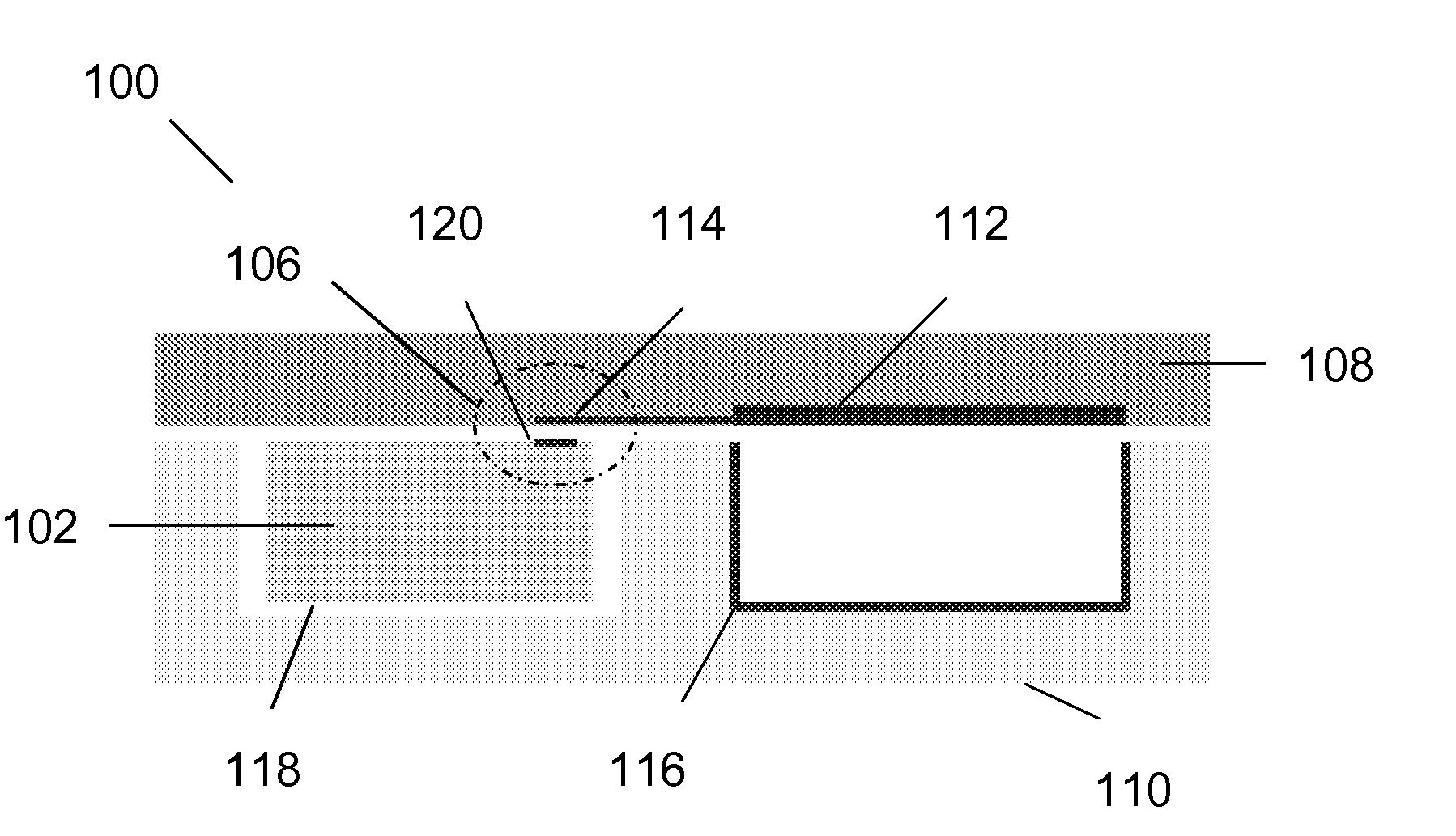
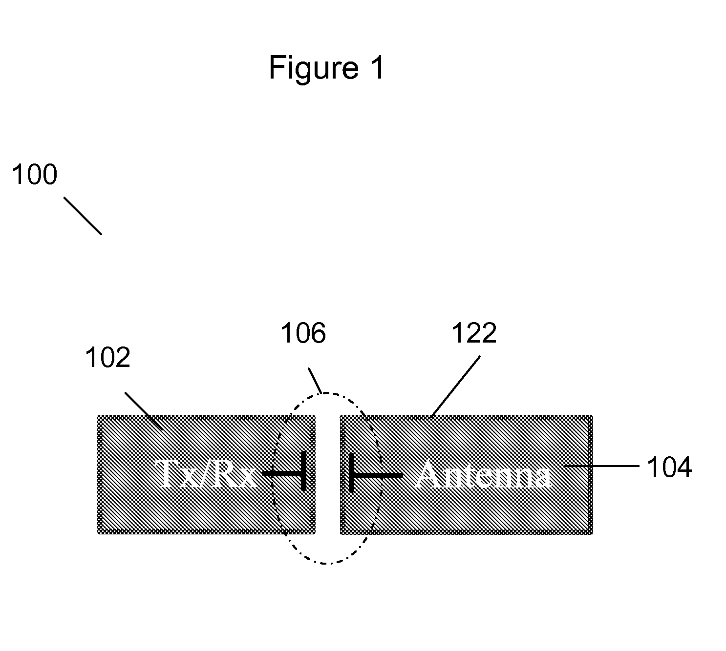
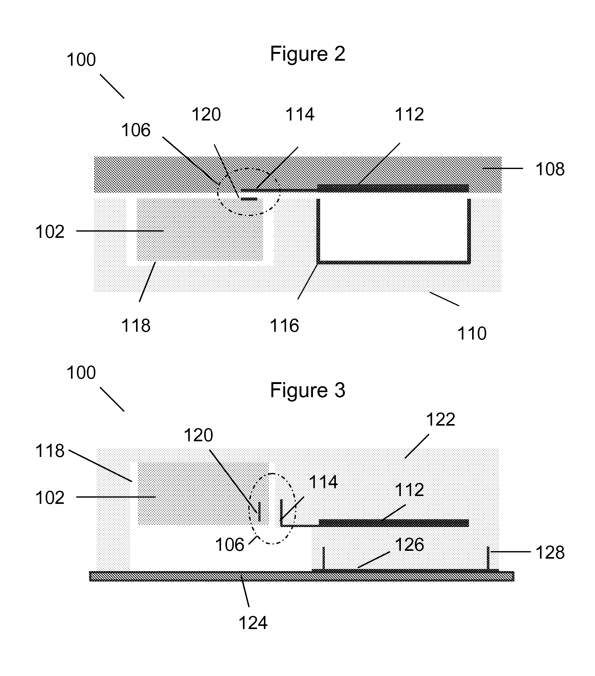
[0031]An embodiment of the invention provides an integrated circuit structure. The integrated circuit structure includes a first package substrate comprising a radiating element, the radiating element having a radiating element connection extending from the radiating element; a first chip positioned adjacent to the radiating element connection, the first chip having a first chip connection on a surface of the first chip; wherein the first chip connection forms a capacitive coupling with the radiating element connection. The integrated circuit structure may be termed an integrated circuit package antenna (ICPA) and the first package substrate may be termed an antenna-in-package (A...


PUM


Abstract

An integrated circuit structure is disclosed. The integrated circuit structure includes a first package substrate including a radiating element, the radiating element having a radiating element connection extending from the radiating element. The integrated circuit structure further includes a first chip positioned adjacent to the radiating element connection, the first chip having a first chip connection on a surface of the first chip, wherein the first chip connection forms a capacitive coupling with the radiating element connection. A method of forming an integrated circuit structure is also disclosed.

Description

[0001]The present application claims the benefit of U.S. provisional application 60 / 893,963 (filed on 9 Mar. 2007), the entire contents of which are incorporated herein by reference for all purposes.FIELD OF THE INVENTION[0002]Embodiments of the invention relate generally to integrated circuit structures and a method of forming the same. Specifically, embodiments of the invention relate to an integrated circuit package antenna (ICPA) and an antenna-in-package (AiP).BACKGROUND OF THE INVENTION[0003]Traditionally, millimetre-wave (MMW), sub-millimeter-wave (sub-MMW), and Terahertz radios are implemented with multiple chips fabricated in III-V semiconductor technologies. As devices used can generate larger output power, the requirement for the transmission loss from the radio frequency (RF) output to the antenna input is relaxed. When a radio having a transmitter (Tx) and receiver (Rx) uses multi-chip module technology, the MMW antenna may be connected to the Tx or Rx RF output by a co...

Claims


Application Information

Patent Timeline
Patent Type & Authority Applications(United States)
IPC IPC(8): H01L23/552H01L21/50
CPCH01L23/48H01L23/66H01L25/0655H01L2223/6677H01L2924/09701H01L2924/3011H01L2924/0002H01Q1/38H01Q13/08H01L2924/00H01L2224/16227H01L2924/3025H01Q1/2283
Inventor ZHANG, YUE PINGSUN, MEI
Owner NANYANG TECH UNIV
Why Eureka
Try Eureka