LED package having an array of light emitting cells coupled in series

a technology of led packages and light emitting cells, which is applied in the field of led package, can solve the problems of complicated coupling process, increased installation cost of leds, and difficulty in using leds for general illumination at home, and achieves the effect of improving the photometric efficiency of light emitting cells, simplifying the process of fabricating a package, and facilitating mass production

Inactive Publication Date: 2010-09-09
SEOUL SEMICONDUCTOR
View PDF30 Cites 35 Cited by
  • Summary
  • Abstract
  • Description
  • Claims
  • Application Information

AI Technical Summary

Benefits of technology

[0024]Moreover, the LED package may further comprise a pair of lead frames spaced apart from each other, and a heat sink. The package body supports the pair of lead frames and the heat sink. The package body may have an opening for exposing a portion of each of the lead frames and an upper portion of the heat sink. Meanwhile, the LED chip is mounted on the heat sink. By employing the heat sink, heat generated from the LED chip can be easily dissipated.
[0044]According to the present invention, it is possible to provide an LED package and an LED lamp, which can be driven using an AC power source without an external AC / DC converter and thus can be miniaturized. Further, since light emitting cells formed on a single substrate are employed, the process of fabricating a package can be simplified and thus is advantageous to mass production. Moreover, since generated heat can be easily dissipated by employing the heat sink, the photometric efficiency of the light emitting cells can be improved. Furthermore, since the heat sink can be prevented from being separated from the package body, it is possible to provide an LED package that is stable in view of its structure.

Problems solved by technology

With the use of an AC / DC converter together with LEDs, installation costs of LEDs increase, which makes it difficult to use the LEDs for general illumination at home.
However, since the LED lamp have serially coupled LEDs with individual LED chips mounted thereon, the process of coupling the LEDs is complicated, and the size of the LED is lamp considerably increases since the LEDs occupy a large space.
However, the junction temperature of the LED increases due to the increase of the input electric power.
The increase of the junction temperature of the LED results in decrease of photometric efficiency that represents the degree of conversion of input energy into visual light.

Method used


Image

  • LED package having an array of light emitting cells coupled in series
  • LED package having an array of light emitting cells coupled in series
  • LED package having an array of light emitting cells coupled in series

Examples


Embodiment Construction

[0055]Hereinafter, preferred embodiments of the present invention will be described in is detail with reference to the accompanying drawings. The following embodiments are provided only for illustrative purposes so that those skilled in the art can fully understand the spirit of the present invention. Therefore, the present invention is not limited to the following embodiments but may be implemented in other forms. In the drawings, the widths, lengths, thicknesses and the like of elements are exaggerated for convenience of illustration. Like reference numerals indicate like elements throughout the specification and drawings.

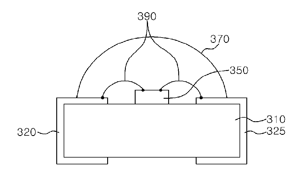
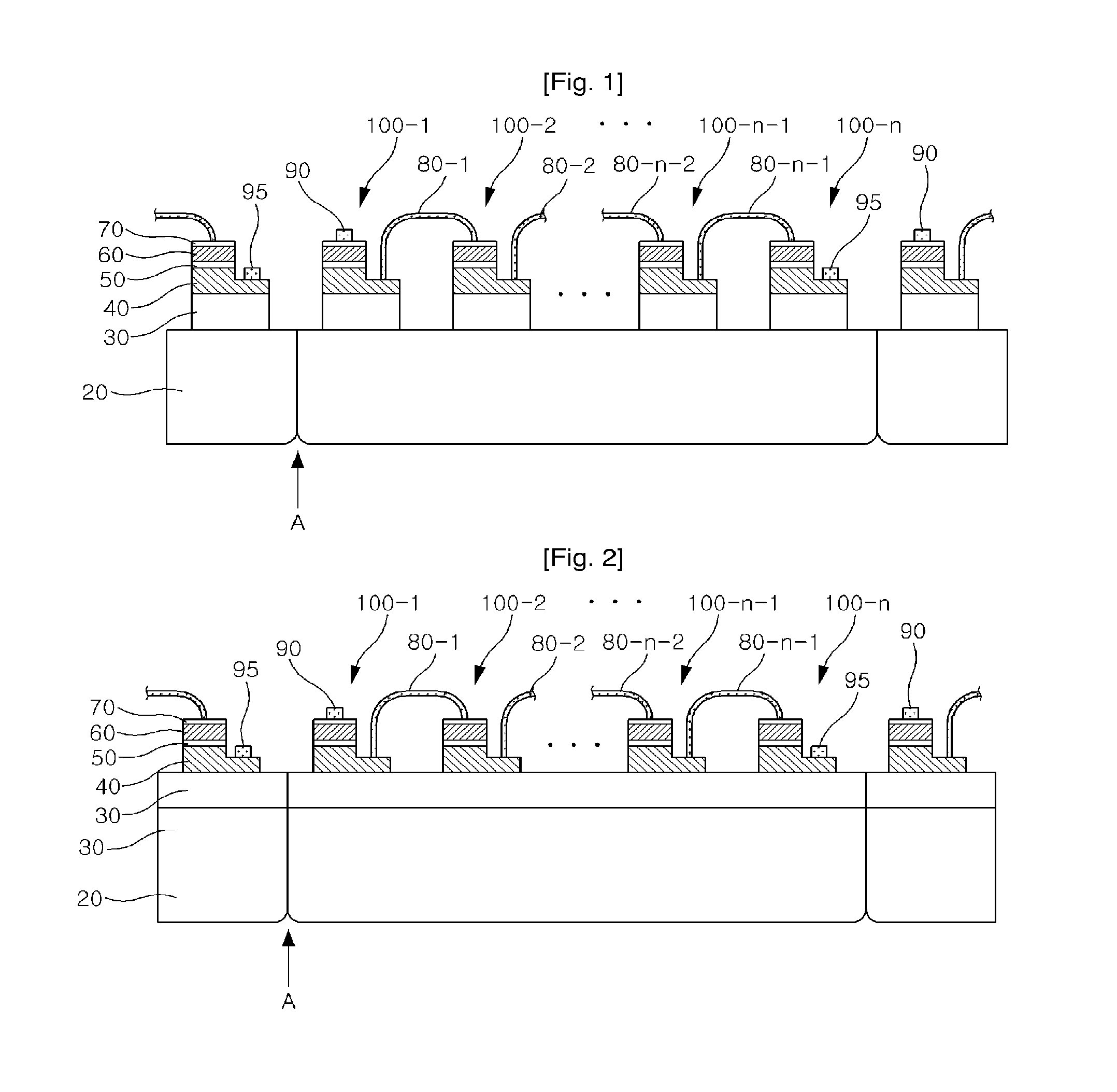
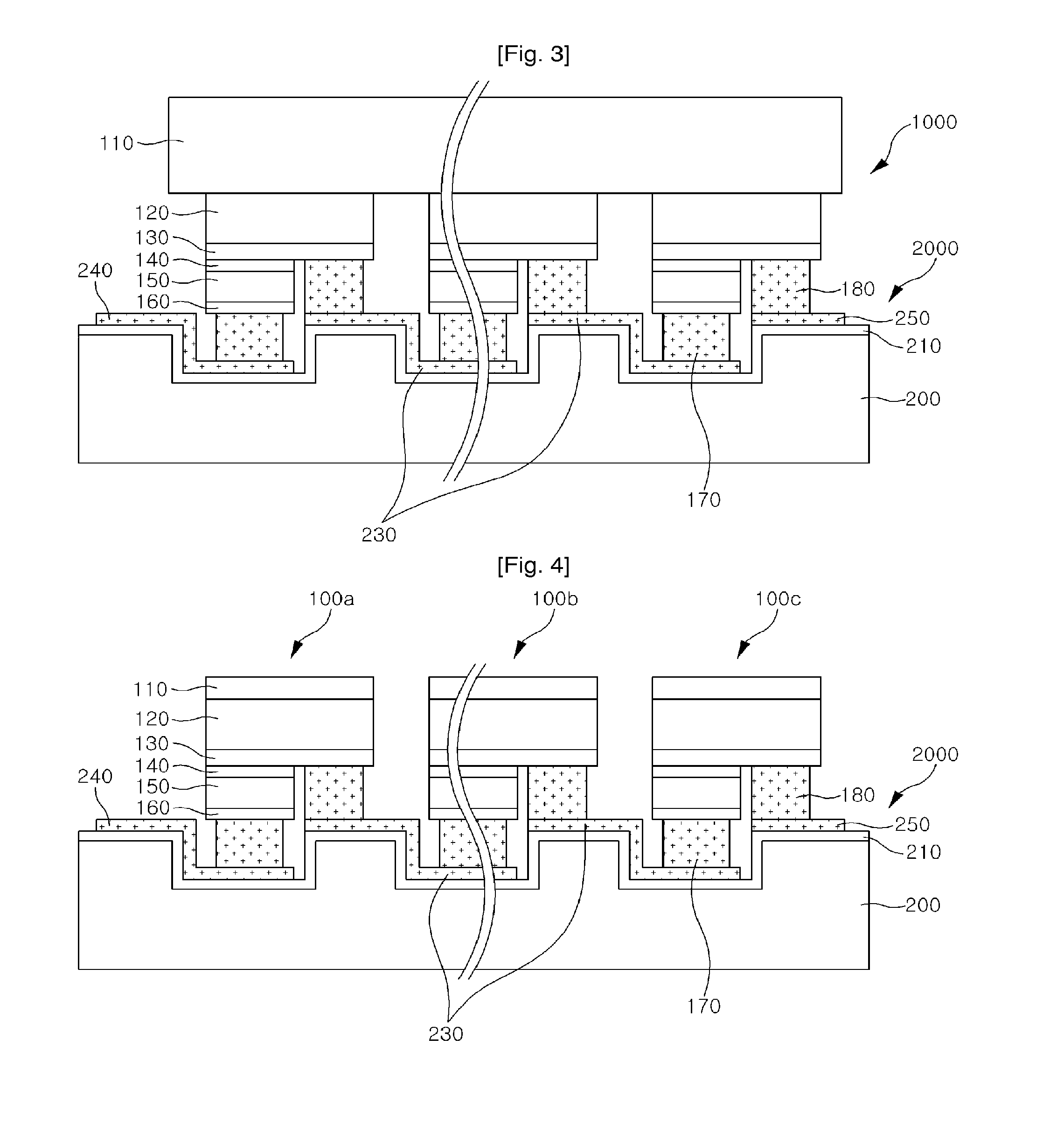
[0056]A light emitting diode (LED) package according to the present invention includes an array of light emitting cells coupled in series. FIGS. 1 to 5 are sectional views illustrating arrays of light emitting cells coupled in series, which are applicable to embodiments of the present invention. Here, FIGS. 1 and 2 are sectional views illustrating LED chips each ...


PUM


Abstract

Disclosed is a light emitting diode (LED) package having an array of light emitting cells coupled in series. The LED package comprises a package body and an LED chip mounted on the package body. The LED chip has an array of light emitting cells coupled in series. Since the LED chip having the array of light emitting cells coupled in series is mounted on the LED package, it can be driven directly using an AC power source.

Description

CROSS-REFERENCE TO RELATED APPLICATIONS[0001]This application is a continuation of U.S. patent application Ser. No. 11 / 908,112 filed Sep. 7, 2007, which is a U.S. national stage application of PCT International Application No. PCT / KR2005 / 003565, filed on Oct. 26, 2005, and claims priority from and the benefit of Korean Patent Application No. 10-2005-0026090, filed on Mar. 29, 2005; Korean Patent Application No. 10-2005-026078, filed on Mar. 29, 2005, Korean Patent Application No. 10-2005-0026067, filed Mar. 29, 2005; Korean Patent Application No. 10-2005-0026108, filed Mar. 29, 2005; and Korean Patent Application No. 10-2005-0020377, filed Mar. 11, 2005 which are hereby incorporated by reference for all purposes as if fully set forth herein.BACKGROUND OF THE INVENTION[0002]1. Field of the Invention[0003]The present invention relates to a light emitting diode (LED) package, and more particularly, to an LED package having an array of light emitting cells coupled in series, which can b...

Claims


Application Information

Patent Timeline
Patent Type & Authority Applications(United States)
IPC IPC(8): H01L33/62H01L33/64H01L33/52H01L33/50H01L33/58H01L33/60
CPCF21K9/00H01L27/153H01L33/486H01L33/62H01L33/642H01L2224/48247H01L2224/48091H01L2224/48137H01L2924/01322H01L2924/12041H01L2924/00014H01L33/36H01L33/60H01L33/20
Inventor LEE, CHUNG HOONLEE, KEON YOUNGKIM, HONG SANKIM, DAE WONCHOI, HYUCK JUNG
Owner SEOUL SEMICONDUCTOR
Why Eureka
Try Eureka