Package for housing light-emitting element, light-emitting apparatus and illumination apparatus

a technology of light-emitting elements and packaging, which is applied in the field of packaging, can solve the problems of poor wavelength conversion efficiency, deterioration of optical power, brightness, color rendering, and inability to readily excite fluorescent materials present in specular reflection directions, and achieve the effect of effectively suppressing light leakage, increasing radiation light intensity, and improving heat dissipation properties

Inactive Publication Date: 2005-06-23
KYOCERA CORP
View PDF8 Cites 128 Cited by
  • Summary
  • Abstract
  • Description
  • Claims
  • Application Information

AI Technical Summary

Benefits of technology

[0096] According to the invention, the base body has a wiring conductor formed so as to extend from its upper surface to outer surface. The reflection member has, around the mounting portion, a through hole drilled all the way through from the upper principal surface to the lower principal surface thereof so as to lie below the optical path line. The electrode of the light-emitting element and the wiring conductor formed on the upper surface of the base body are electrically connected to each other by means of a wire inserted through the through hole. In this construction, direct light emitted from the light-emitting element is reflected from the reflection surface above the through hole drilled in the reflection member for inserting thereinto the wire. Thus, the direct light can be effectively prevented from being directed into and absorbed in the through hole, thereby increasing the radiation light intensity.
[0097] Moreover, the light-emitting element is, at its entire lower surface, joined to the mounting portion of the reflection member. This make it possible to transmit the heat emanating from the light-emitting element to the reflection member satisfactorily and thereby improve the heat-dissipation property.
[0098] Furthermore, it is possible to effectively suppress that light leaks through the through hole for inserting the wire therethrough which through hole is formed in the reflection member and is absorbed into the base body, by setting the average particle diameter of the crystal grains contained in ceramics to a range of 1 to 5 μm to improve the reflectivity of the base body.
[0099] According to the invention, the through hole is filled with an insulative paste containing insulative light-reflecting particles. In this way, even though the light emitted from the light-emitting element or the fluorescent materials is directed into the through hole, the light can be effectively reflected upward from the light-reflecting particles. Hence, the light-emitting apparatus is capable of offering satisfactory optical characteristics such as high radiation intensity, on-axis luminous intensity, brightness, and color rendering.
[0100] According to the invention, the illumination apparatus of the invention is constructed by setting up the light-emitting apparatus of the invention in a predetermined arrangement. In this construction, light emission is effected by exploiting recombination of electrons in the light-emitting element formed of a semiconductor. Thus, there is provided a compact illumination apparatus that has the advantage, in terms of power saving and long lifetime, over a conventional illumination apparatus for affecting light emission through electrical discharge. As a result, variation in the center wavelength of the light emitted from the light emitting element can be suppressed; wherefore the illumination apparatus will succeed in irradiating light with stable radiation light intensity and angle (luminous intensity distribution) for a longer period of time, and in avoiding color unevenness and unbalanced illumination distribution on a to-be-irradiated surface.
[0101] Moreover, by setting up the light-emitting apparatus of the invention as a light source in a predetermined arrangement, followed by arranging around the light-emitting apparatus an optical component optically designed in a given configuration such as a reflection jig, an optical lens, or a light diffusion plate, it is possible to realize an illumination apparatus capable of emitting light with given luminous intensity distribution.

Problems solved by technology

In this case, the fluorescent materials other than fluorescent materials present in a specular reflection direction cannot be excited readily.
That is, wavelength conversion is effected mainly by a part of the fluorescent materials, which leads to poor wavelength conversion efficiency.
This gives rise to a problem of optical power, brightness, and color rendering being deteriorated.
As a result, the light-emitting apparatus fails to provide desired optical power, as well as recently-demanded satisfactory light takeoff efficiency.
Further, in a case where the base body 12 has its upper surface coated with a metal film to prevent light absorption on the substrate 12, the metal film needs to be formed by means of plating or vapor deposition, which leads to an undesirable increase in the manufacturing process steps and manufacturing cost.
The remaining heat thus causes significant degradation of the light-emitting efficiency of the light-emitting element 14.
This makes it impossible to enhance the optical power.
By contrast, when the fluorescent material content is reduced, the wavelength conversion efficiency will be decreased, and thus light having a desired wavelength cannot be obtained.
As a result, enhancement of the optical power becomes impossible.
This gives rise to a problem of the radiation intensity of the light omitted from the light-emitting apparatus being lower.
This gives rise to a problem that the radiation intensity of the light emitted from the light-emitting apparatus cannot be maintained with stability.
This gives rise to a problem of the radiation intensity, brightness, and color rendering of the light emitted from the light-emitting apparatus being deteriorated.
This gives rise to a problem of the radiation intensity, brightness, and color rendering of the light omitted from the light-emitting apparatus being deteriorated.
This causes the bonding strength between the conductor layer 27 and the light-emitting element 25 to decrease, which may result in difficulty in maintaining the steadfast fixation between the conductor layer 27 and the light-emitting element 25 for a longer period of time.
As a result, inconveniently, there arises a problem such as a break between the electrode 26 of the light-emitting element 25 and the conductor layer 27.
This makes it difficult to achieve a longer service life in the light emitting apparatus.
This makes it impossible to obtain stable radiation intensity.
This gives rise to a problem that the radiation intensity which is proportional to an input current cannot be obtained.
Also, this gives rise to a problem that stable radiation intensity cannot be obtained due to variation in light emission wavelength which is predicted to be due to heat.
This makes it impossible to enhance the radiation intensity.
By contrast, if the fluorescent material 34 content is reduced, the wavelength conversion efficiency will be decreased, and thus light having a desired wavelength cannot be obtained.
As a result, enhancement of the radiation intensity becomes impossible.
This gives rise to problems of the radiation angle being varied and the radiation intensity being lowered.

Method used


Image

  • Package for housing light-emitting element, light-emitting apparatus and illumination apparatus
  • Package for housing light-emitting element, light-emitting apparatus and illumination apparatus
  • Package for housing light-emitting element, light-emitting apparatus and illumination apparatus

Examples


example 1

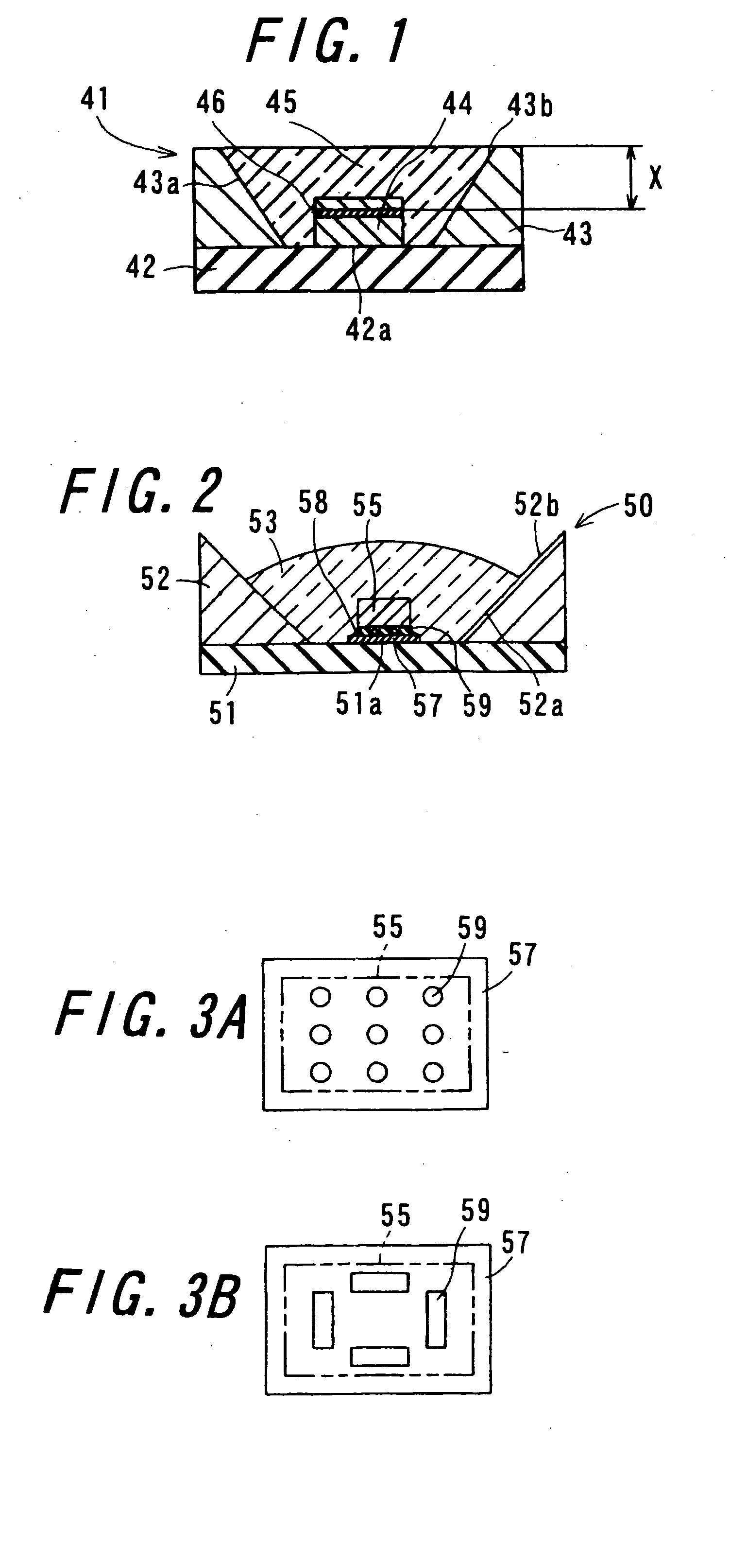
[0288] Hereinafter, a description will be given as to an implemented example of the light-emitting apparatus 41 according to the first embodiment of the invention.

[0289] At first, as the base body 42, an alumina ceramic substrate made of crystalline particles having different diameters was prepared. Then, around the mounting portion 42a for mounting thereon the light-emitting element 44 was formed a wiring conductor for electrically connecting the light-emitting element 44 to the external electric circuit board through an internal wiring line formed within the base body 42. Note that the wiring conductor formed on the upper surface of the base body 42 was shaped into a 0.1 mm-diameter circular pad with use of a metallized layer made of Mo—Mn powder. The wiring conductor has its surface coated with a 3 μm-thick Ni plating layer and a 2 μm thick Au plating layer successively. Moreover, the internal wiring line formed within the base body 42 was constituted by an electrical connection...

example 2

[0295] Next, samples of the light-emitting apparatus 41 were fabricated. The samples, of which each has the same structure as that of the above-stated implemented example, are identical in structure with one another, but differ from one another in an average particle diameter of the ceramic crystal grains as observed after the sintering of the base body 42:1 (μm); 5 (μm); and 10 (μm). Then, the total light beams (optical power) with respect to the load current for the light-emitting element 44 were measured. Note that the light-emitting apparatuses 41 were individually mounted in heat sinks that are identical in cooling capability with one another. The optical power was measured by means of integrating sphere. The results are listed in FIG. 27.

[0296] As will be understood from FIG. 27, given the load current for the light-emitting element 44 of 20 (mA), i.e. rated current and rated voltage of 3.4 (V), then the light-emitting apparatus 41 having the average particle diameter of the ...

example 3

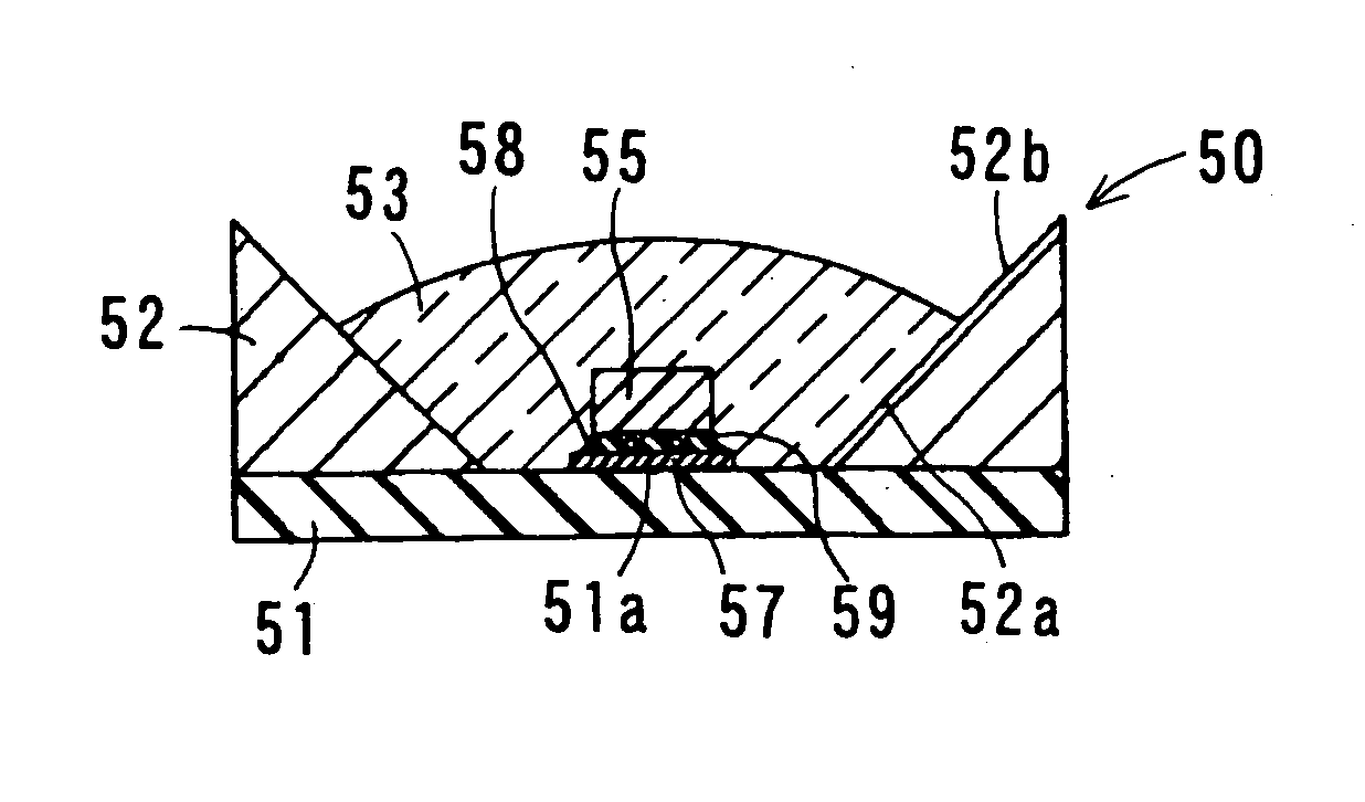
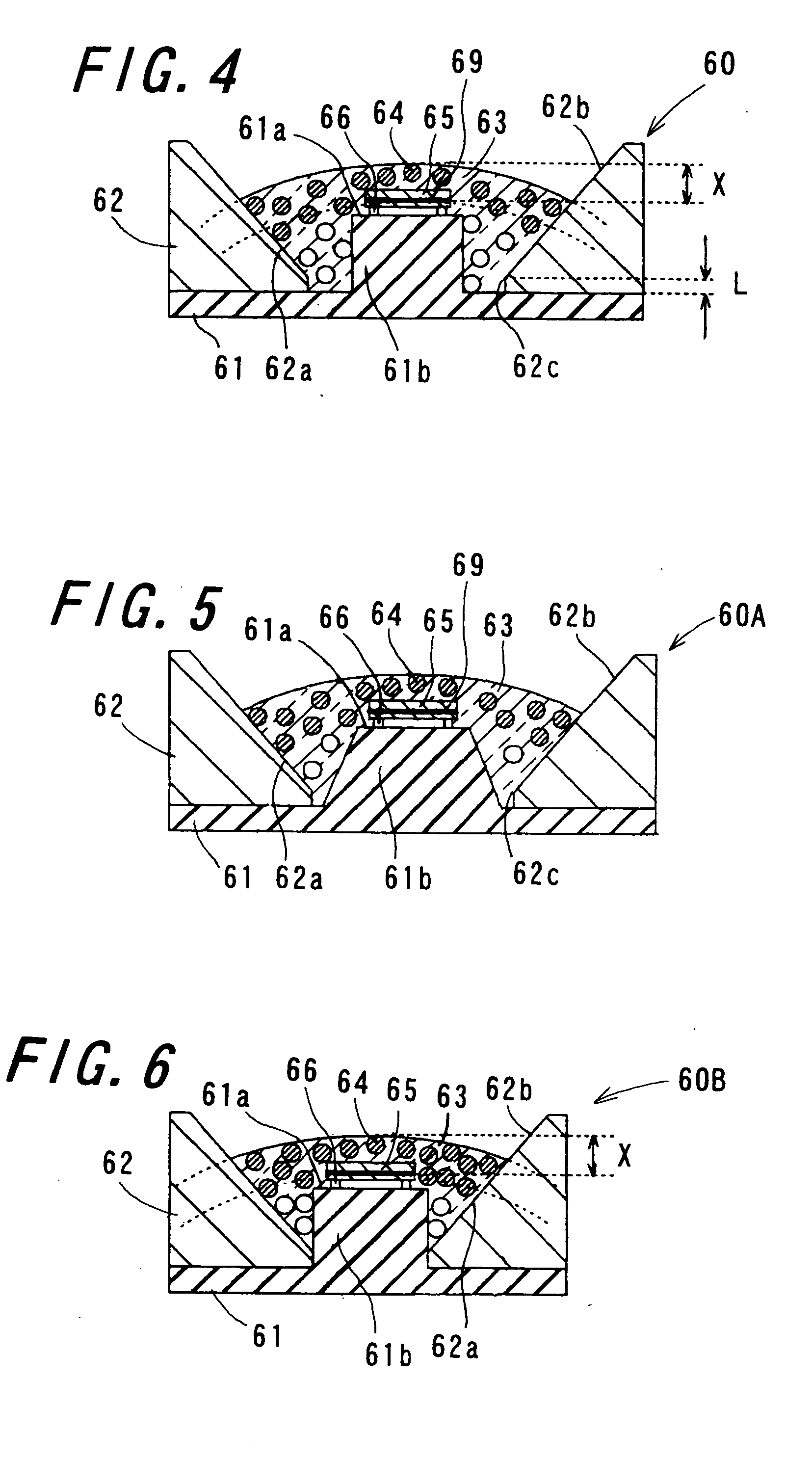
[0300] Hereinafter, an implemented example of the light-emitting apparatus 60c according to the sixth embodiment of the invention will be described with reference to FIG. 7.

[0301] At first, as the base body 61, an alumina ceramic substrate was prepared. Note that the base body 61 has the convexity 61b with a mounting portion 61a formed integrally therewith. The upper surface of the mounting portion 61A and the upper surface of the base body 61 excluding a part of the mounting portion 61a were arranged parallel to each other.

[0302] The base body 61 is composed of a cylindrically-shaped plate of 0.8 mm in diameter and 0.5 mm in thickness and a cylindrically-shaped convexity 61b of 0.4 mm in diameter and any given value in thickness. The convexity 61b if formed at the center of the upper surface of the cylindrically-shaped plate.

[0303] The convexity 61b includes the mounting portion 61a for mounting thereon the light-emitting element 65. Formed on the mounting portion 61a is an elec...


PUM


Abstract

A light-emitting apparatus provides a ceramic-made base body, a frame body, a light-emitting element, a conductor layer and a light-transmitting member. The base body has on its upper surface a mounting portion for the light-emitting element. The frame body is joined to the upper surface of the base body so as to surround the mounting portion, with its inner peripheral surface shaped into a reflection surface. The wiring conductor has its one end formed on the upper surface of the base body and electrically connected to the light-emitting element, and has another end led to a side or lower surface of the base body. The light-transmitting member is disposed inside the frame body so as to cover the light-emitting element, which contains fluorescent materials for performing wavelength conversion. The base body is so designed that ceramic crystal grains range in average particle diameter from 1 to 5 μm.

Description

BACKGROUND OF THE INVENTION [0001] 1. Field of the Invention [0002] The present invention relates to a package for housing a light-emitting element; a light-emitting apparatus; and an illumination apparatus, in particular, to a package for housing a light-emitting element; a light-emitting apparatus; and an illumination apparatus which allow light emitted from a light-emitting element and wavelength-converted by fluorescent materials to radiate out. [0003] 2. Description of the Related Art [0004]FIG. 31 shows a light-emitting apparatus 11 according to a first related art in which light such as near-ultraviolet light of blue-color light emitted from a light-emitting element 14, for example a light emitting diode (LED), is wavelength-converted by a plurality of fluorescent materials (not shown) which are excited by the light emitted from the light-emitting element and generate fluorescence of different colors such as red, green, blue, and yellow, so as to be emitted therefrom as white...

Claims


Application Information

Patent Timeline
Patent Type & Authority Applications(United States)
IPC IPC(8): H01L33/38H01L33/48H01L33/50H01L33/60H01L33/62
CPCH01L33/486H01L33/508H01L33/60H01L33/62H01L2933/0091H01L2224/48091B41J2/455H01L2224/73265H01L2224/45144H01L2924/1815H01L2924/00014H01L2924/00
Inventor URAYA, MITSUGUSAKUMOTO, DAISUKEMIYAKE, AKIRASEKINE, FUMIAKIMORI, YUKIYANAGISAWA, MITSUOSHIBAYAMA, HIROSHIMATSUURA, SHINGO
Owner KYOCERA CORP
Why Eureka
Try Eureka