Circuit for Measuring Magnitude of Electrostatic Discharge (ESD) Events for Semiconductor Chip Bonding

a technology of electrostatic discharge and semiconductor chip, which is applied in the direction of testing circuits, semiconductor/solid-state device testing/measurement, instruments, etc., can solve the problems of tens to hundreds of square microns, damage to parts of the path that cannot withstand the energy associated with the discharge, and large area consumed by structures

Inactive Publication Date: 2010-09-09
QUALCOMM INC
View PDF11 Cites 22 Cited by
  • Summary
  • Abstract
  • Description
  • Claims
  • Application Information

AI Technical Summary

Problems solved by technology

Any part of this path that is unable to withstand the energy associated with the discharge sustains damage.
These structures consume a considerable amount of area (tens to hundreds of square microns for each ESD buffer) on the substrate that could otherwise be used for active circuitry.
The resultant stacked IC has a significantly higher density of devices, but also requires significantly more complex manufacturing methods than an individual IC.
Moreover, no standard procedures for handling stacked ICs have been implemented.

Method used


Image

  • Circuit for Measuring Magnitude of Electrostatic Discharge (ESD) Events for Semiconductor Chip Bonding
  • Circuit for Measuring Magnitude of Electrostatic Discharge (ESD) Events for Semiconductor Chip Bonding
  • Circuit for Measuring Magnitude of Electrostatic Discharge (ESD) Events for Semiconductor Chip Bonding

Examples


Embodiment Construction

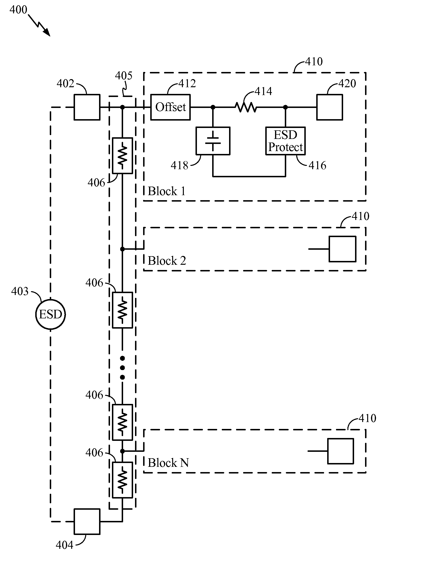
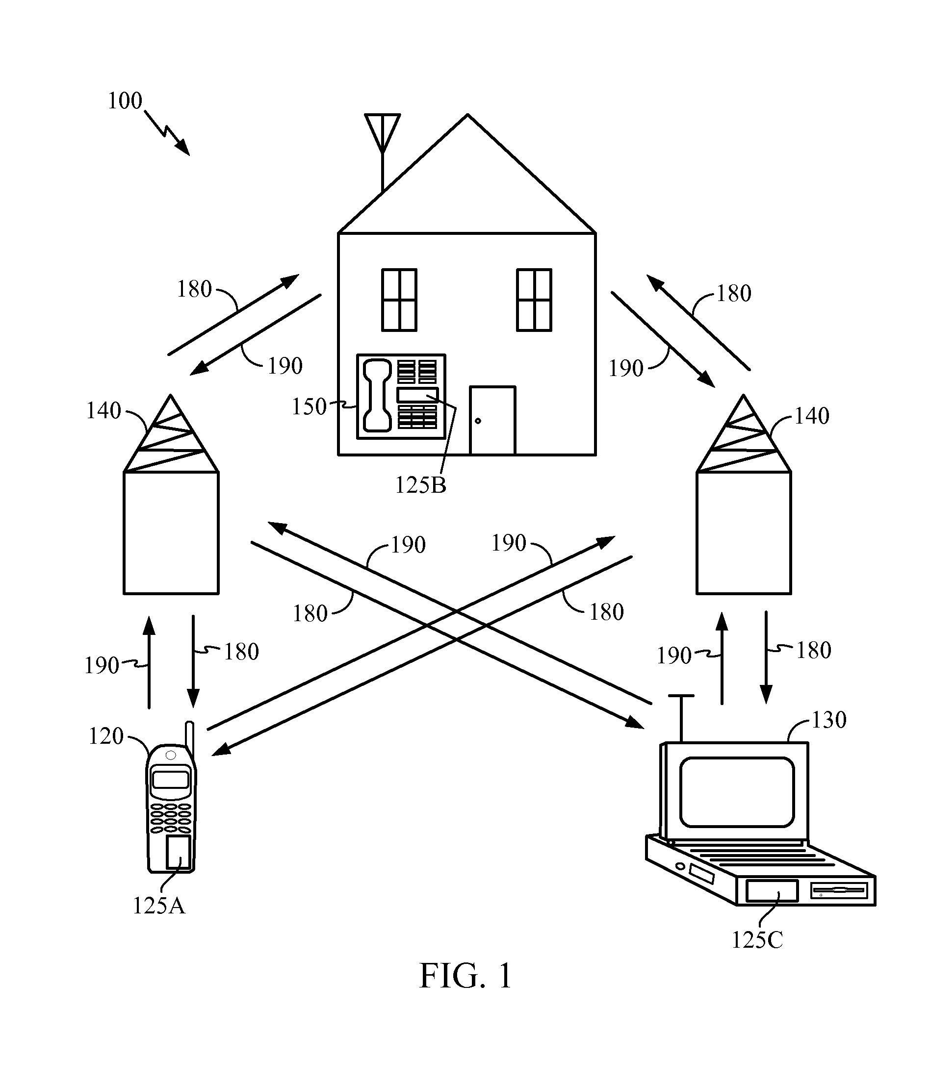
[0025]FIG. 1 is a block diagram showing an exemplary wireless communication system 100 in which an embodiment of the disclosure may be advantageously employed. For purposes of illustration, FIG. 1 shows three remote units 120, 130, and 150 and two base stations 140. It will be recognized that wireless communication systems may have many more remote units and base stations. Remote units 120, 130, and 150 include IC devices 125A, 125B and 125C, that include the disclosed ESD recorder. It will be recognized that any device containing an IC may also include the ESD recorder disclosed here, including the base stations, switching devices, and network equipment. FIG. 1 shows forward link signals 180 from the base station 140 to the remote units 120, 130, and 150 and reverse link signals 190 from the remote units 120, 130, and 150 to base stations 140.

[0026]In FIG. 1, remote unit 120 is shown as a mobile telephone, remote unit 130 is shown as a portable computer, and remote unit 150 is show...


PUM


Abstract

A circuit for recording a magnitude of an ESD event during semiconductor assembly includes a voltage divider connected between an input and a ground. The circuit also includes a measurement block having a recorder device. Each measurement block receives current from a segment of the voltage divider. The magnitude of the ESD event is determined based upon a read-out of the measurement devices after the ESD event. The recorder device may be a capacitor that would be damaged during the ESD event. During the ESD event the capacitor may be damaged. Reading out the recorder device determines if the magnitude of the ESD event exceeded a threshold magnitude that damages the capacitor.

Description

CROSS REFERENCE TO RELATED APPLICATION[0001]This application claims the benefit of U.S. Provisional Patent Application No. 61 / 158,505, entitled “A Circuit For Measuring Magnitude Of Electrostatic Discharge (ESD) Events For Semiconductor Chip Bonding” to WORLEY et al., filed Mar. 9, 2009.TECHNICAL FIELD[0002]The present disclosure generally relates to integrated circuits (ICs). More specifically, the present disclosure relates to IC assembly, and even more specifically to measuring electrostatic discharge (ESD) events in assembled ICs.BACKGROUND[0003]Electrostatic discharge (ESD) events are a common part of everyday life and some of the larger discharges are detectable by the human senses. Smaller discharges go unnoticed by human senses because the ratio of discharge strength to surface area over which the discharge occurs is very small.[0004]Integrated circuits (ICs) have been shrinking at an incredible rate over past decades. By way of example, transistors in ICs have shrunk to 32 ...

Claims


Application Information

Patent Timeline
Patent Type & Authority Applications(United States)
IPC IPC(8): G01R19/00G01R31/26
CPCH01L22/34G01R31/002H01L2224/16225G01R29/12G01R31/14G01R31/26H01L22/00
Inventor WORLEY, EUGENE R.HENDERSON, BRIAN MATTHEW
Owner QUALCOMM INC
Why Eureka
Try Eureka