White light emitting diode package and method of making the same

a technology of light-emitting diodes and white led, which is applied in the direction of basic electric elements, semiconductor devices, electrical equipment, etc., can solve the problems of great light absorption loss of led, and achieve the effect of reducing light absorption loss and improving light outpu

Inactive Publication Date: 2010-09-16
NEPES LED CORP
View PDF5 Cites 78 Cited by
  • Summary
  • Abstract
  • Description
  • Claims
  • Application Information

AI Technical Summary

Benefits of technology

[0006]The present invention is to solve the above mentioned problem by providing a white LED package and its packaging method, which effectively prevents excited emission from phosphor from going back and hitting LED die and substrate area around LED die, hence enhances white lighting efficiency.
[0007]The technical solution is to use a low refractive index silicone (the second type of silicone encapsulant) to separate the phosphor containing layer from the first type of silicone encapsulant, which is used to cover the LED dies. As the refractive index of the phosphor containing layer is larger than that of the low refractive index silicone (the second type of silicone encapsulant), the light rays emitted by phosphor with an incident angle larger than the critical angle on the interface of the second type of silicone and the phosphor containing layer will be reflected and prevented from going backward to hit the LED die and the substrate area around the LED die, so that less absorption can be ensured and the overall white light output can be improved.
[0009]The effective reflective index of the phosphor containing layer is higher than that of the layer resides directly below the phosphor containing layer to reduce the amount light going backward to hit the LED die and the substrate area around the LED die. This thus reduces light absorption loss and improves light output.

Problems solved by technology

In this method, the LED suffers a great light absorption loss when the emitted light from the phosphor propagates backwardly into the LED die or to the substrate area around the LED die because of close proximity between phosphor and the LED die.

Method used


Image

  • White light emitting diode package and method of making the same
  • White light emitting diode package and method of making the same

Examples


Embodiment Construction

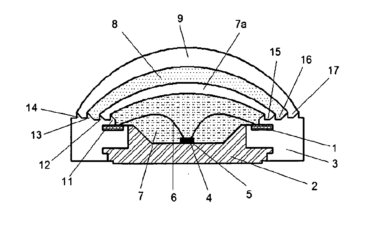
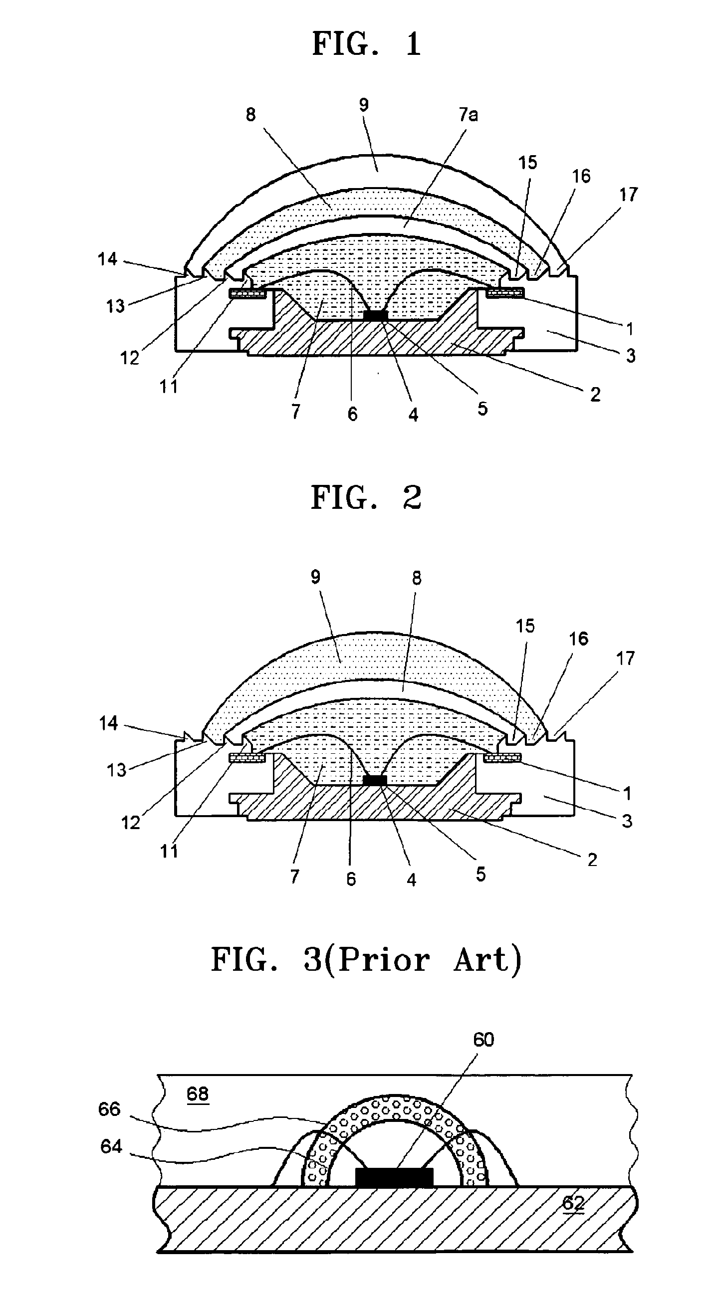
[0013]This invention is related to a light emitting diode (LED) device; more specifically it is related to a white LED package structure and its packaging methods.

[0014]The LED package of the invention has a multilayered encapsulation structure that is formed by utilizing surface tension method and leadframe structure providing surface tension phenomenon.

[0015]The LED package of the invention as shown in FIG. 1 comprises of metal electrodes 1, a heat dissipation base 2, a PPA plastic 3 to fix the metal electrodes 1 and the heat dissipation base 2 together, an LED die 4, a die attach material 5, gold wires 6, silicone encapsulation layers 7 and 7a, a phosphor containing layer 8, an optical lens 9, sharp edge ring-alike structures 11, 12, 13, and 14 with a tilted inner surface, and ring-alike grooves 15, 16, and 17 formed between sharp edge ring-alike structures.

[0016]As shown in FIG. 1, the LED die 4 is attached onto the heat dissipation base 2 by using a die attach material 5, such ...


PUM


Abstract

A white light emitting diode (LED) package with multilayered encapsulation structure and the packaging methods are disclosed. The white LED package structure includes metal electrodes, a heat dissipation base, a PPA plastic for fixing the electrodes and the heat dissipation base together, at least one LED die, a die attaching material, gold wires for electrically connecting the LED die to the electrodes, a first type of silicone encapsulant, a second type of silicone encapsulant, and a phosphor containing layer. The invention utilizes a low-refractive index silicone (the second type of silicone encapsulant) to separate the phosphor containing layer away from the first type of silicone, which covers the LED die, to prevent / reduce emitted light going backward and hitting the LED die.

Description

BACK GROUND OF INVENTION[0001]1. Field of the Invention[0002]This invention is related to a light emitting diode (LED) device; more specifically it is related to a white LED package structure and its packaging methods.[0003]2. Background Art[0004]As a semiconductor lighting device, LED has superior advantages over traditional lighting devices, such as incandescent bulb and fluorescent tube, with a longer life time, a more compact size, a lower applied voltage source, no mercury pollution, and a more energy saving property. Therefore it is called the first option of the green lighting sources, and has already been widely used in signal light, display, and LCD backlighting. There is also a trend for the LED to replace the incandescent and fluorescent in general illumination area.[0005]In a traditional method for making a white LED, the phosphor containing layer is directly dispensed onto and cover the surfaces of a blue or UV LED die so that the excited light from the phosphor with va...

Claims


Application Information

Patent Timeline
Patent Type & Authority Applications(United States)
IPC IPC(8): H01L33/00
CPCH01L33/483H01L33/507H01L33/54H01L33/58H01L2224/8592H01L2224/45144H01L2224/48247H01L2224/48091H01L2924/00014H01L2924/00H01L2924/181
Inventor TRAN, NGUYEN THE
Owner NEPES LED CORP
Why Eureka
Try Eureka