Hybrid STI Gap-Filling Approach

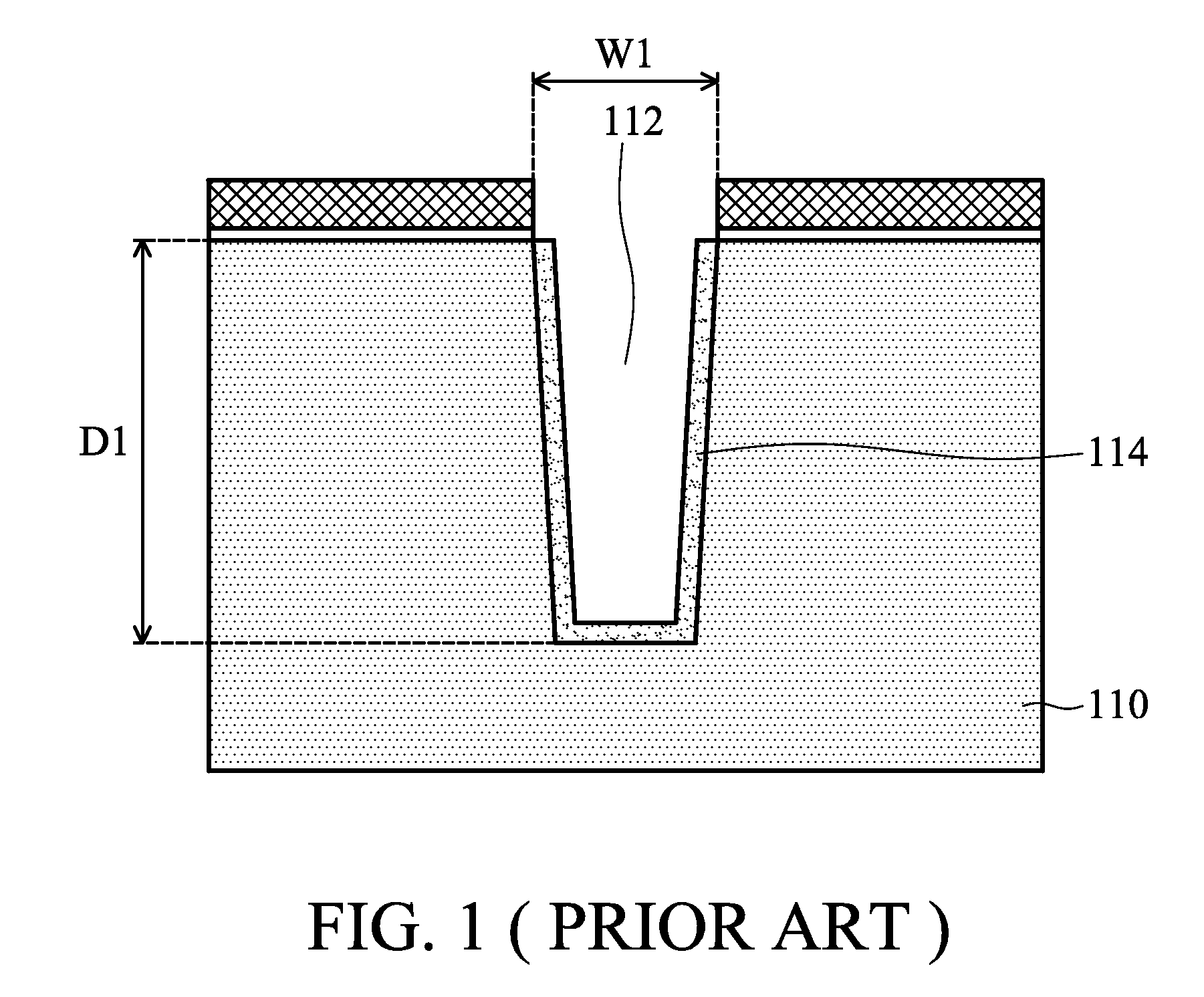
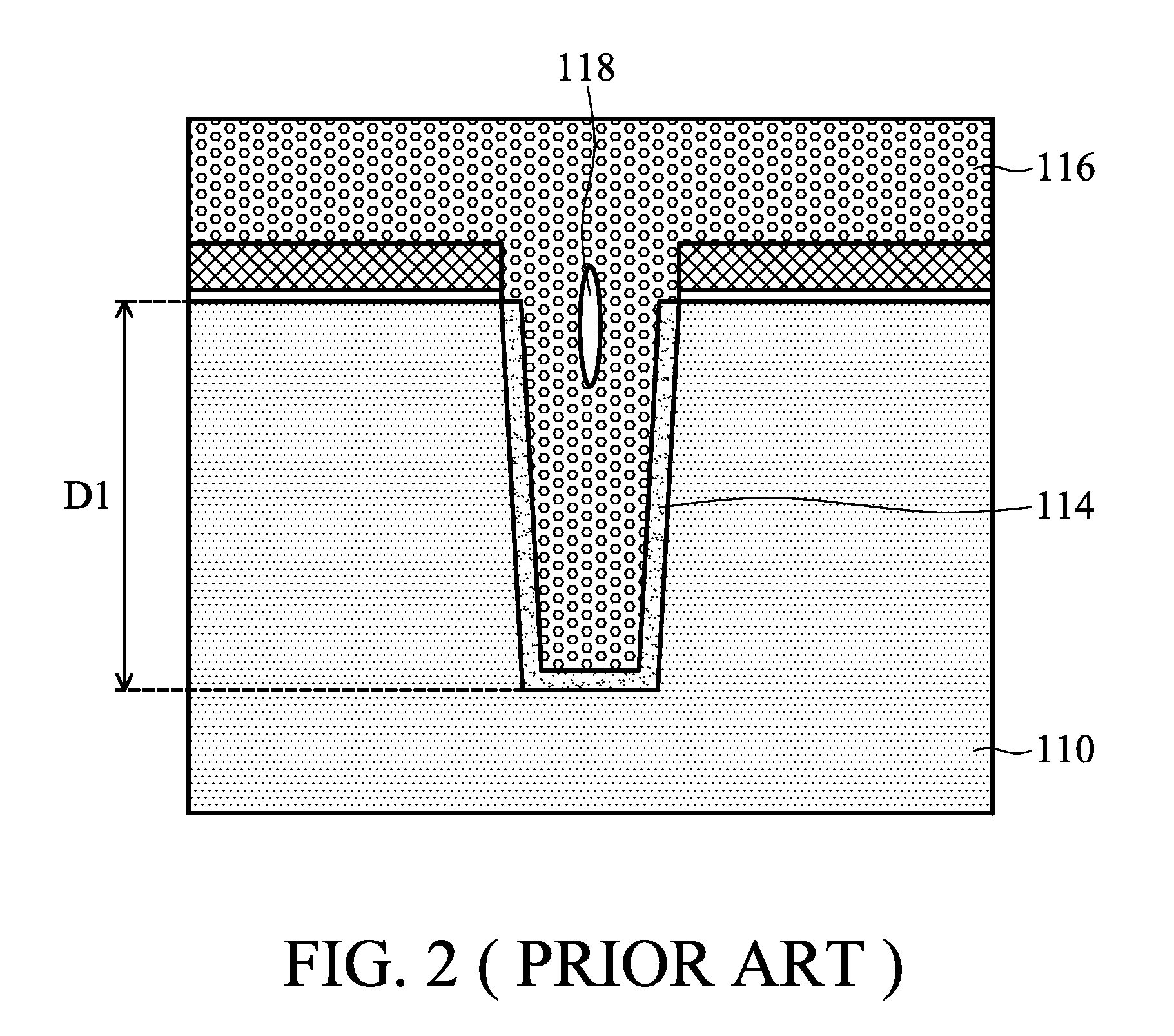
a technology of gap-filling and hybrid sti, applied in the direction of basic electric elements, electrical equipment, semiconductor devices, etc., can solve the problems of bridging, void formation, and even shorting of integrated circuits in some circumstances, and increase the aspect ratio

Active Publication Date: 2010-09-16
TAIWAN SEMICON MFG CO LTD
View PDF35 Cites 64 Cited by
  • Summary
  • Abstract
  • Description
  • Claims
  • Application Information

AI Technical Summary

Benefits of technology

[0009]In accordance with another aspect of the present invention, a method of forming an integrated circuit structure includes providing a semiconductor substrate having a top surface; forming an opening extending from the top surface into the semiconductor substrate; and performing a first deposition step using a first deposition method to fill a first dielectric material into the opening. The first dielectric material is recessed to form a first recess in the opening and having a first depth. A second deposition step is performed to fill the opening with a second dielectric material. The second deposition step is performed using a second deposition method different from the first deposition method. The second dielectric material is recessed to form a second recess in the opening, wherein the second recess has a second depth smaller than the first depth.
[0010]In accordance with yet another aspect of the present invention, a method of forming an integrated circuit structure includes providing a semiconductor substrate having a top surface; forming an opening extending from the top surface into the semiconductor substrate; and performing a first deposition step to fill a first dielectric material into the opening. The first dielectric material is recessed to form a first recess. A second deposition step is performed to fill the first recess with a second dielectric material using high-density plasma (HDP). An annealing is performed to the second dielectric material. The second dielectric material is then planarized, followed by recessing the second dielectric material.

Problems solved by technology

The increase in the aspect ratio causes problems.
Referring to FIG. 2, in the filling of the opening, the high aspect ratio will adversely result in the formation of void 117, which is a result of the pre-mature sealing in the top region of oxide 116.
In subsequent process steps, conductive materials, such as polysilicon, may be filled into the opening, causing the bridging, and even the shorting, of integrated circuits in some circumstances.
The weak portions may be damaged by the CMP processes, which in turn cause voids as a result of the CMP.
Accordingly, the existing gap-filling techniques can only fill gaps having aspect ratios less than 7.0 without causing voids.
In addition to the above-discussed problem, the conventional gap-filling methods also incur problems in the formation of fin field-effect transistors (FinFETs).

Method used


Image

  • Hybrid STI Gap-Filling Approach
  • Hybrid STI Gap-Filling Approach
  • Hybrid STI Gap-Filling Approach

Examples


Embodiment Construction

[0018]The making and using of the embodiments of the present invention are discussed in detail below. It should be appreciated, however, that the embodiments provide many applicable inventive concepts that can be embodied in a wide variety of specific contexts. The specific embodiments discussed are merely illustrative of specific ways to make and use the invention and do not limit the scope of the invention.

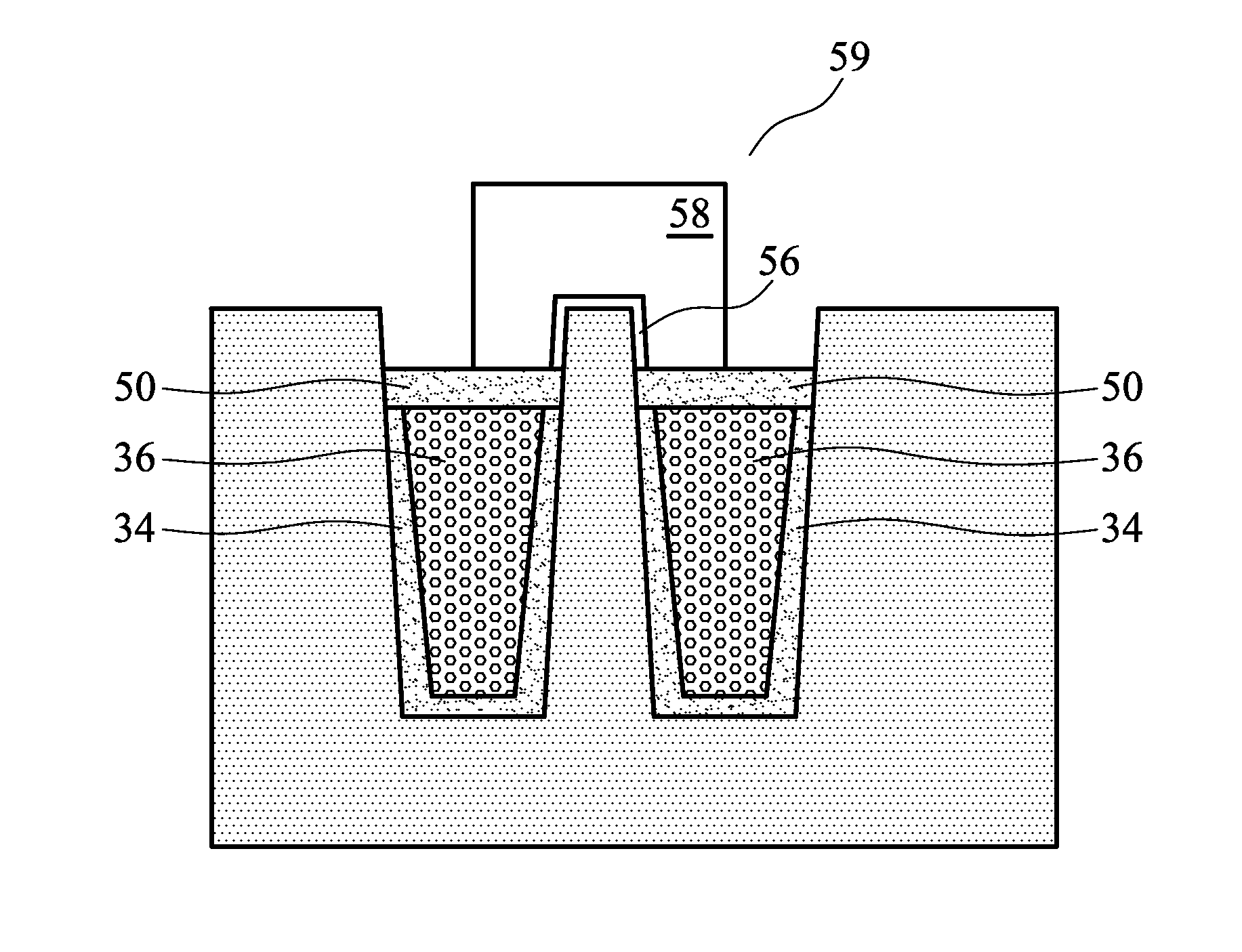
[0019]A novel method for forming a shallow trench isolation (STI) region and a fin field-effect transistor (FinFET) is provided. The intermediate stages in the manufacturing of an embodiment are illustrated. The variations of the embodiment are discussed. Throughout the various views and illustrative embodiments of the present invention, like reference numbers are used to designate like elements.

[0020]Referring to FIG. 5, semiconductor substrate 20 is provided. In an embodiment, semiconductor substrate 20 includes silicon. Other commonly used materials, such as carbon, germanium...


PUM


Abstract

A method of forming an integrated circuit structure includes providing a semiconductor substrate including a top surface; forming an opening extending from the top surface into the semiconductor substrate; and performing a first deposition step to fill a first dielectric material into the opening. The first dielectric material is then recessed. A second deposition step is performed to fill a remaining portion of the opening with a second dielectric material. The second dielectric material is denser than the first dielectric material. The second dielectric material is recessed until a top surface of the second dielectric material is lower than the top surface of the semiconductor substrate.

Description

[0001]This application claims the benefit of U.S. Provisional Application No. 61 / 160,635 filed on Mar. 16, 2009, entitled “Hybrid STI Gap-Filling Approach,” which application is hereby incorporated herein by reference.TECHNICAL FIELD[0002]This invention relates generally to integrated circuits and more particularly to structures and manufacturing methods of shallow trench isolation (STI) regions and semiconductor fins.BACKGROUND[0003]Modern integrated circuits are formed on the surfaces of semiconductor substrates, which are mostly silicon substrates. Semiconductor devices are isolated from each other by isolation structures formed at the surfaces of the respective semiconductor substrates. The isolation structures include field oxides and shallow trench isolation (STI) regions.[0004]With the down-scaling of integrated circuits, STI regions are increasingly used as the isolation structures. FIGS. 1 and 2 illustrate intermediate stages in the formation of an STI region. First, as sho...

Claims


Application Information

Patent Timeline
Patent Type & Authority Applications(United States)
IPC IPC(8): H01L29/78H01L21/762H01L21/28
CPCH01L21/76232H01L29/785H01L29/66795
Inventor CHEN, NENG-KUOTSAI, CHENG-YUANTZENG, KUO-HWA
Owner TAIWAN SEMICON MFG CO LTD
Why Eureka
Try Eureka