

Semiconductor device having a conductive bump
- Summary
- Abstract
- Description
- Claims
- Application Information
AI Technical Summary
Benefits of technology
Problems solved by technology
Method used
Image

Examples
embodiment 1
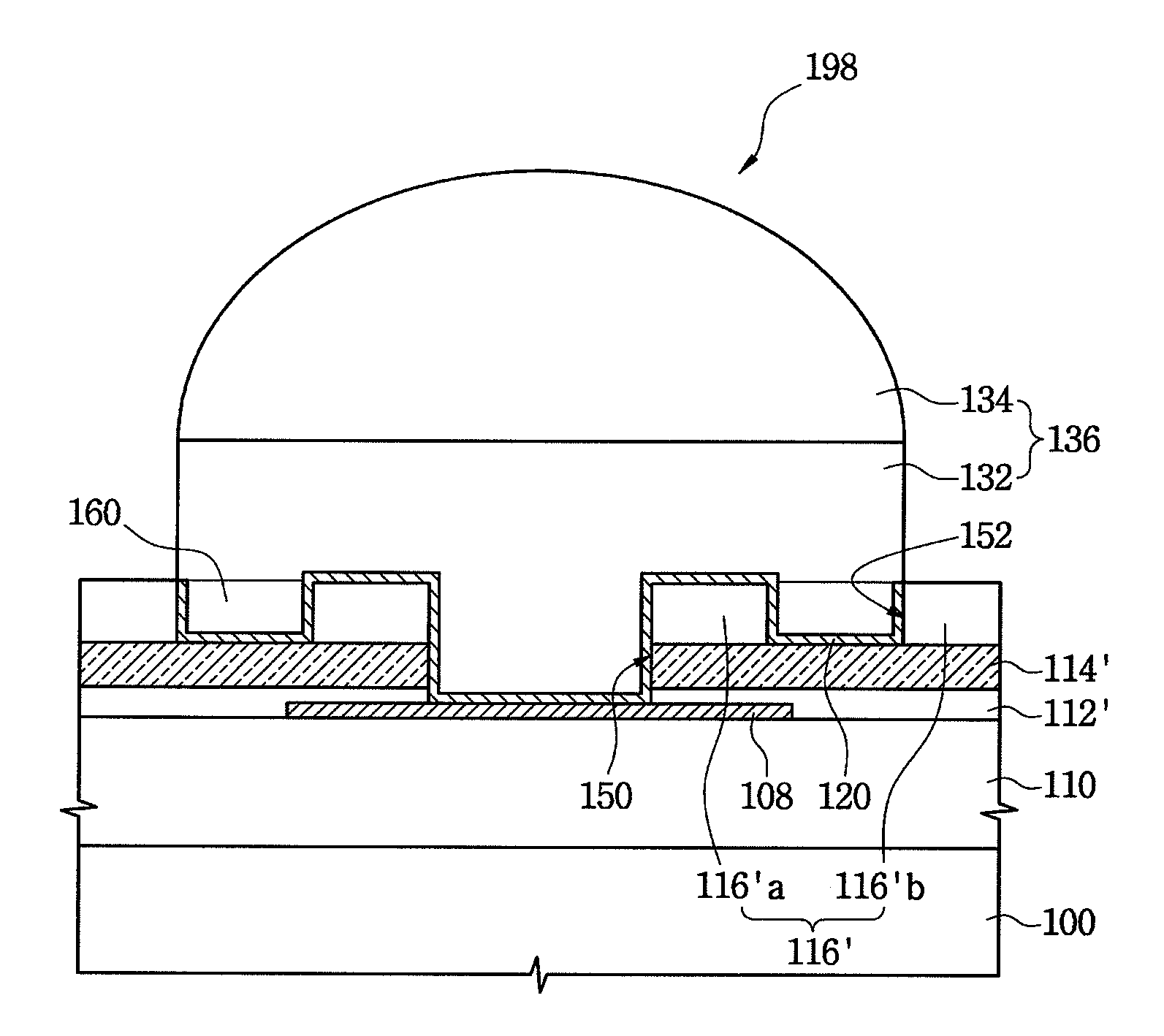
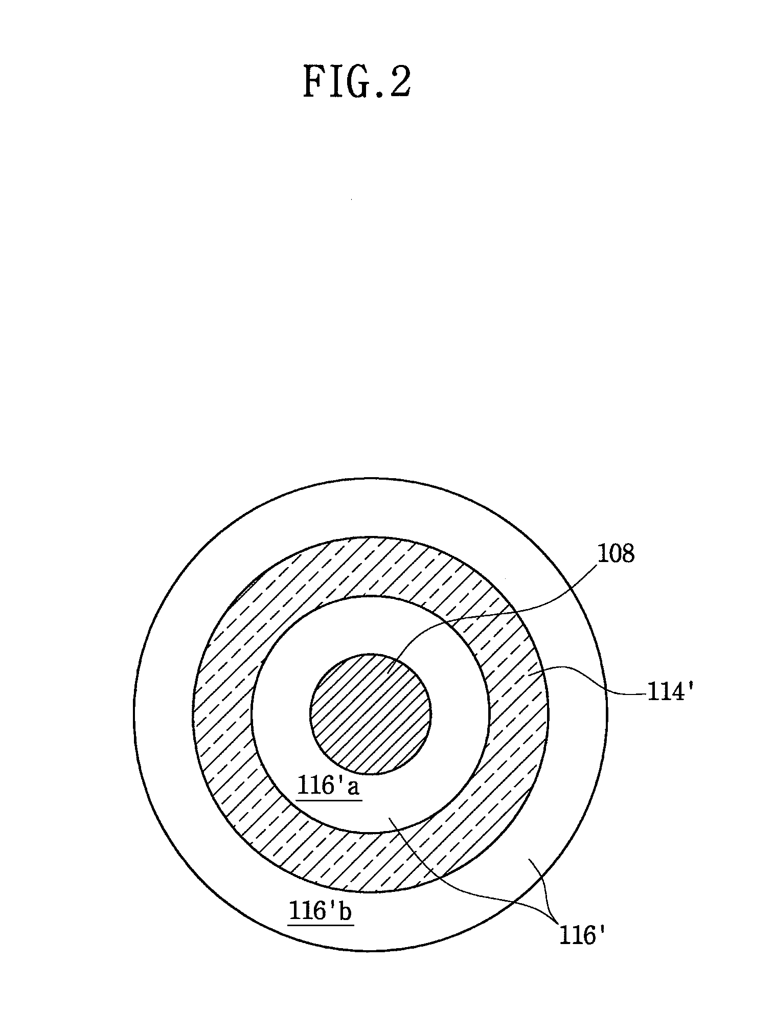
[0038]FIG. 1 is a cross-sectional view of a semiconductor device 198 for a flip-chip bonding process according to a first example embodiment, which mainly illustrates a solder land region in which a conductive ball or conductive bump such as a solder bump 136 may be formed. Also, FIG. 2 is a plan view of the semiconductor device 198 of FIG. 1, in which the solder bump 136 and a metal barrier layer 120 are omitted to facilitate the understanding of a planar structure of the semiconductor device.
[0039]Referring to FIGS. 1 and 2, the semiconductor device 198 for the flip-chip bonding process may include a semiconductor substrate 100, a bonding pad 108 disposed on the semiconductor substrate 100, and the solder bump 136 used to electrically connect the semiconductor device 198 with a printed circuit board (PCB) (not shown). Also, a passivation layer 112′, a buffer layer 114′, and an insulating layer 116′ may be sequentially stacked on the semiconductor substrate 100. The insulating laye...
embodiment 2
[0063]Hereinafter, a semiconductor device 298 for a flip-chip bonding process according to other example embodiments will be described with reference to FIGS. 5, 6, and 7A through 7E. For the sake of brevity, a detailed description of the same components as in Embodiment 1 will be omitted.
[0064]The semiconductor device 298 for a flip-chip bonding process according to the present example embodiments may include a semiconductor substrate 200, a bonding pad 208 disposed on the semiconductor substrate 200, and a conductive bump such as a solder bump 236 used to electrically connect the semiconductor device with a PCB substrate (not shown). Also, a passivation layer 212′, a buffer layer 214′, and an insulating layer 216′ may be sequentially stacked on the semiconductor substrate 200. The insulating layer 216′, the buffer layer 214′, and the passivation layer 212′ may include a first recess 250 exposing the bonding pad 208. Also, the insulating layer 216′ may further include a stick 260 t...
embodiment 3
[0080]FIG. 8 is a cross-sectional view of a semiconductor device 398 having a bump 336 with a stick or protrusion 360 according to a third example embodiment, and FIGS. 9A through 9C are cross-sectional views illustrating a method of fabricating the semiconductor device 398 of FIG. 8.
[0081]Referring to FIG. 8, the semiconductor device 398 for a flip-chip bonding process according to the present example embodiments may include a semiconductor substrate 300, a bonding pad 308 disposed on the semiconductor substrate 300, and a conductive bump, e.g., a solder bump 336 used to electrically connect the semiconductor device 398 with a PCB substrate (not shown). Also, a passivation layer 312′, a buffer layer 314′, and an insulating layer 316′ may be sequentially stacked on the semiconductor substrate 300. The insulating layer 316′, the buffer layer 314′, and the passivation layer 312′ may include a first recess 350 exposing the bonding pad 308. A stick 360 may be obtained by filling a secon...
PUM
 Abstract
Description
Claims
Application Information