Imageing element and display

a technology of image elements and display devices, applied in the field of optical imaging elements, can solve the problems of increasing the size of the display device itself, increasing the depth dimension of the optical system, and increasing the size of the device, so as to reduce the thickness, simplify the configuration, and reduce the cost

Active Publication Date: 2010-09-16
NAT INST OF INFORMATION & COMM TECH
View PDF7 Cites 45 Cited by
  • Summary
  • Abstract
  • Description
  • Claims
  • Application Information

AI Technical Summary

Benefits of technology

[0025]As recited above, according to the present invention, it is possible to form a real image in air of a three or two dimensional image of an actual object or a displayed image having three or two dimensions, respectively, and to view the real image at an angle from a direction diagonal to an element surface, while enabling a simplified configuration, cost reductions, and a thickness reduction.

Problems solved by technology

However, in order to respond to demands to ensure an appropriate viewing angle, optical elements must have large width dimensions; and on the other hand, it is difficult to use an optical element having a short focal distance due to aberrations and other problems, resulting in a larger depth dimension of the optical system.
These considerations unfortunately greatly increase the size of a device that uses the optical element and also result in a larger display device itself.
Moreover, it is difficult to completely eliminate aberrations even in the case where the device is enlarged; the spatial position of the real image unfortunately changes when the viewpoint is changed; and the image of the three dimensional actual object distorts.
However, a real image of a three dimensional actual object cannot be obtained with this technology.

Method used


Image

  • Imageing element and display
  • Imageing element and display
  • Imageing element and display

Examples


Embodiment Construction

[0035]Hereinafter, one exemplary embodiment of the present invention is described with reference to the drawings.

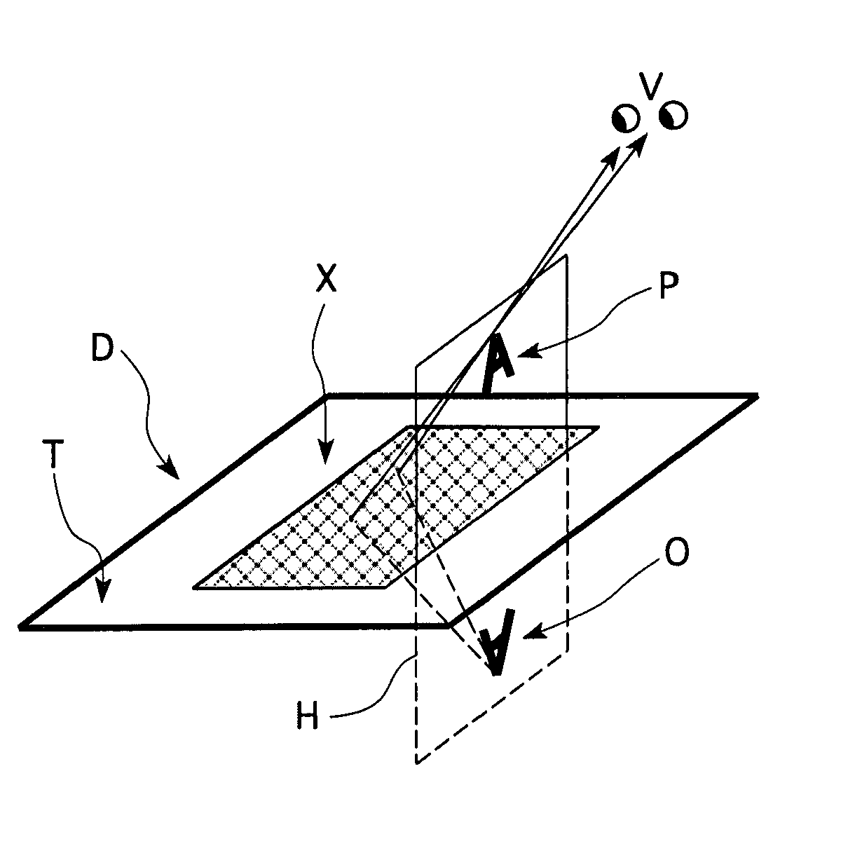
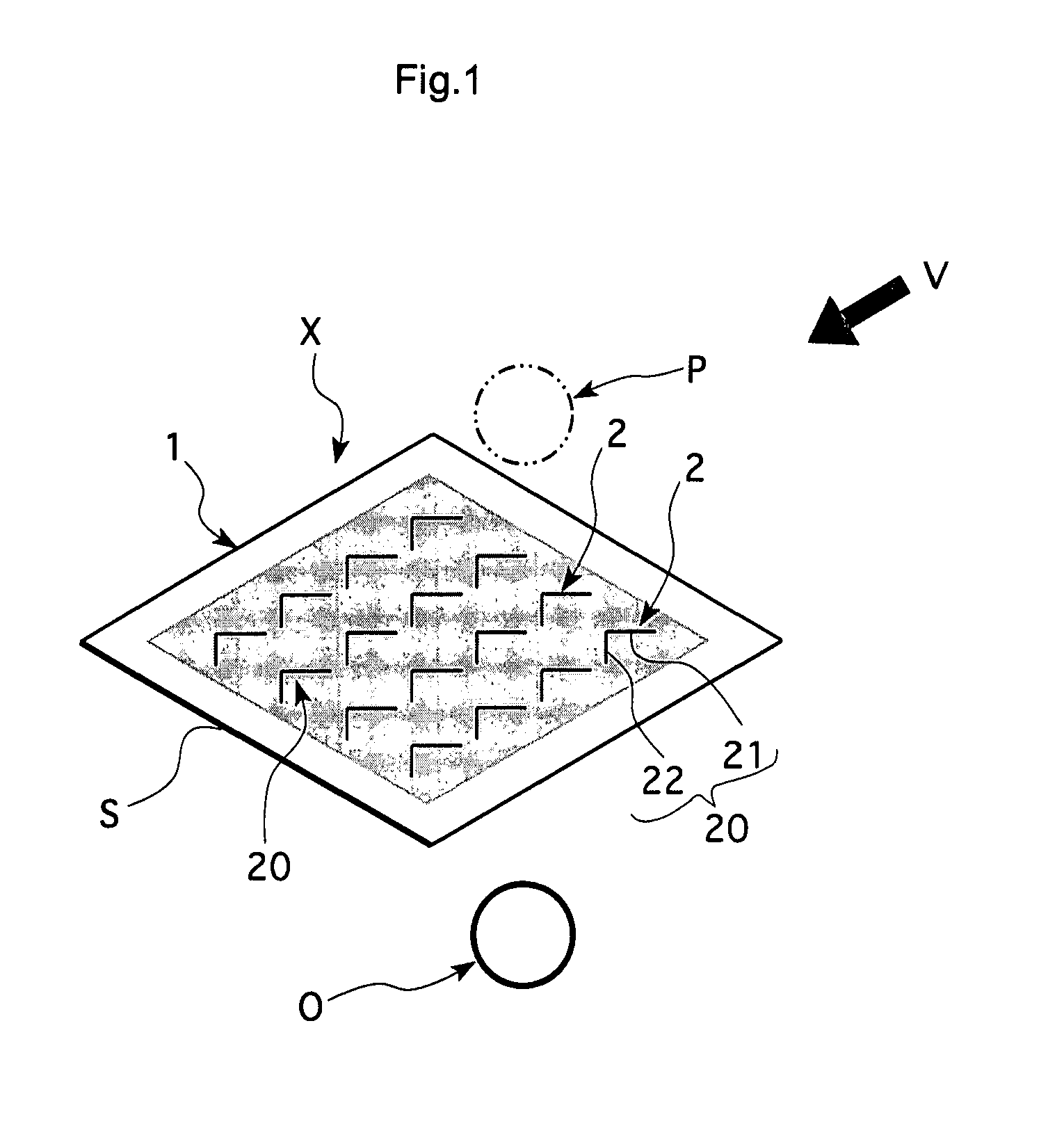
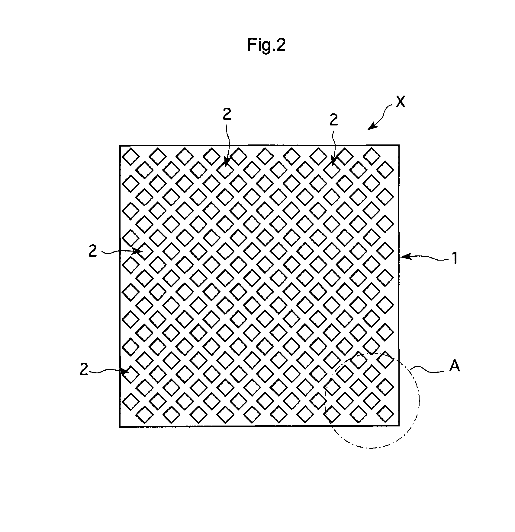
[0036]An optical imaging element X according to this exemplary embodiment functions as a reflective real specular image forming element and arranges, as illustrated in FIG. 1 through FIG. 4, a plurality of unit optical elements 2 including a first interior wall surface and a second interior wall surface made into specular surfaces 21 and 22, respectively, wherein these two interior wall surfaces are orthogonal and pass completely through a substrate 1 in the thickness direction. Hereinafter, the reflective real specular image forming element may be described by adding the reference letter ‘X’ as necessary. In other words, the reflective real specular image forming element X has a function of forming a specular image P as illustrated in FIG. 1. A real image of an object O, arranged in a space on one side of the element surface S (the underside of the substrate 1 in the ill...


PUM


Abstract

As optical elements for bending a light beam when it passes through an element face constituting one plane, a plurality of unit optical elements for reflecting light on one or more mirror surfaces arranged perpendicularly or at an angle nearly perpendicular to the element face are disposed to constitute an optical imaging element. Light emitted from projection object disposed on one side of the element face is reflected on the mirror surface when it passes through the element face so that a real image is formed in a space on the other side of the element face where a physical entity does not exist, thus constituting a display equipped with the optical imaging element. An aerial picture projection system not existing heretofore is also provided.

Description

BACKGROUND OF THE INVENTION[0001]1. Field of the Invention[0002]The present invention relates to an optical imaging element, including an optical element that uses a specular reflection by a micromirror, for forming a real image of an object in air on an opposite side of the element; and a display device including such an optical imaging element.[0003]2. Description of the Related Art[0004]Known conventional optical elements for forming an image of a three dimensional or two dimensional actual object, displayed image, or the like as a real image at a position transferred spatially include aspects that use, for example, convex lenses or concave mirrors. However, in order to respond to demands to ensure an appropriate viewing angle, optical elements must have large width dimensions; and on the other hand, it is difficult to use an optical element having a short focal distance due to aberrations and other problems, resulting in a larger depth dimension of the optical system. These cons...

Claims


Application Information

Patent Timeline
Patent Type & Authority Applications(United States)
IPC IPC(8): G02B27/22G02B27/14
CPCG02B5/08H04N13/0488G02B27/2292G02B5/136G02B30/56H04N13/388
Inventor MAEKAWA, SATOSHI
Owner NAT INST OF INFORMATION & COMM TECH
Why Eureka
Try Eureka