Method for monitoring fabrication parameter

a technology of fabrication parameters and monitoring methods, applied in the field of monitoring fabrication parameters, can solve the problems of difficult to precisely locate the tool, more difficult to further find out which fabrication parameter(s) is/are to be fixed, and the approach may not be precis

US20100233830A1Active Publication Date: 2010-09-16MICRON TECH INC
6 Cites 0 Cited by

Patent Information

Authority / Receiving Office
US · United States
Current Assignee / Owner
Publication Date
2010-09-16

Smart Images

  • Figure 1
    Figure 1
  • Figure 2
    Figure 2
  • Figure 3
    Figure 3
Patent Text Reader

Abstract

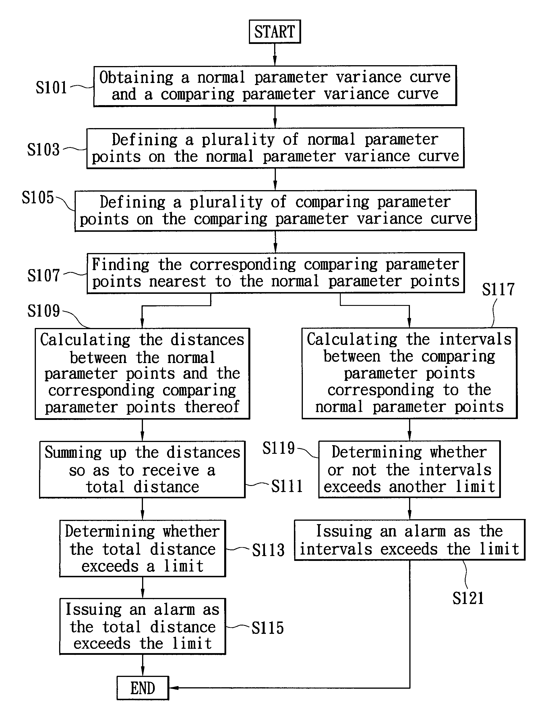
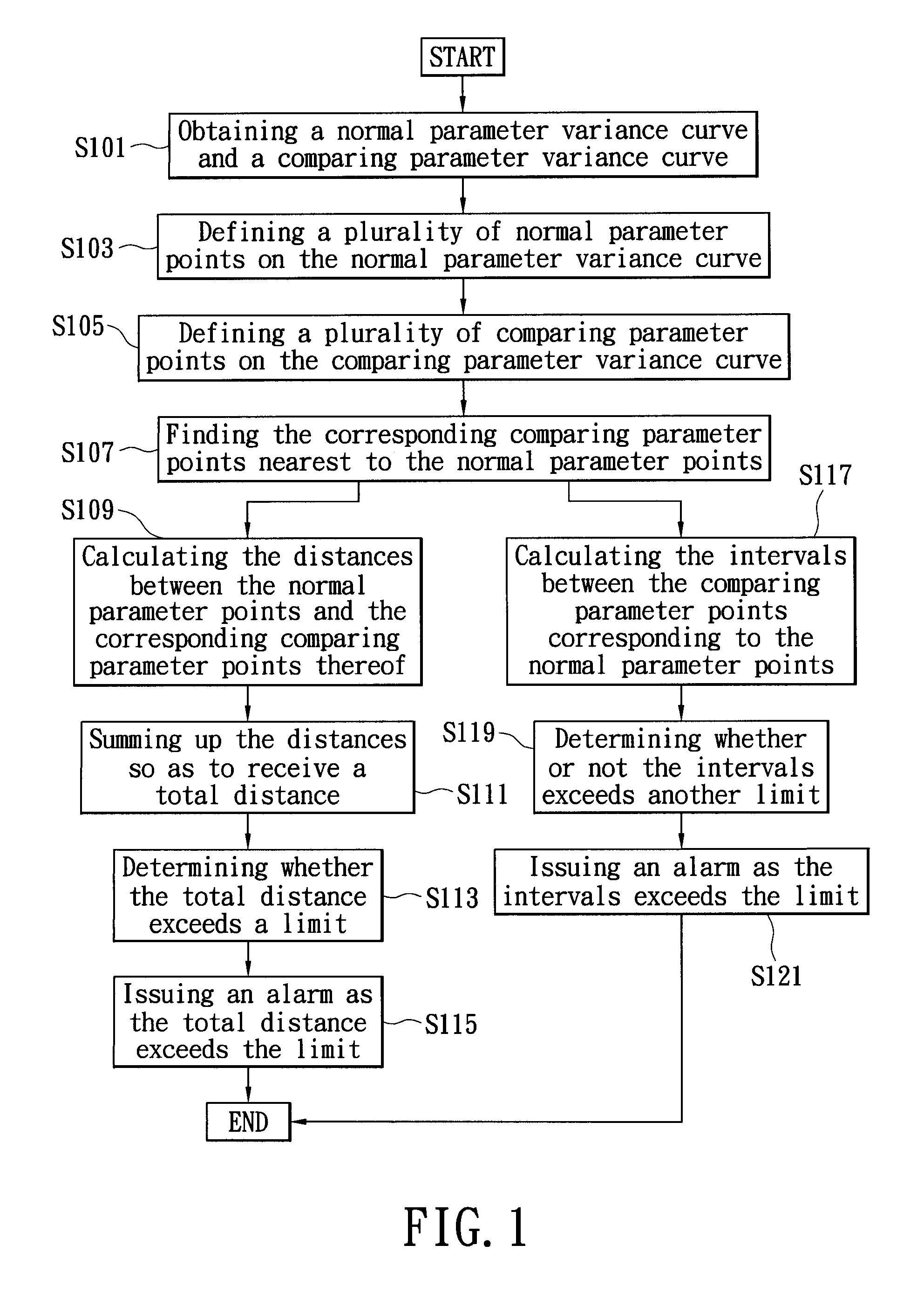
A method for monitoring fabrication parameters comprises steps of: obtaining a normal parameter variance curve and a comparing parameter variance curve; defining a plurality of normal parameter points on the normal parameter variance curve; defining a plurality of comparing parameter points on the comparing parameter variance curve; finding out the corresponding comparing parameter points nearest to the normal parameter points; calculating the distances between the normal parameter points and the corresponding comparing parameter points thereof; summing up the distances so as to receive a total distance; and determining whether or not the total distance exceeds a limit. Via this arrangement, when fabrication parameter of tool is abnormal, it can be efficiently and immediately determined.
Need to check novelty before this filing date? Find Prior Art

Description

BACKGROUND OF THE INVENTION

[0001] 1. Field of the Invention

[0002] The present invention relates to a method for monitoring fabrication parameters; especially, the present invention relates to a method for monitoring fabrication parameters applicable in semiconductor manufacturing.

[0003] 2. Description of Related Art

[0004] In semiconductor manufacturing, each lot of wafers needs to pass through various fabrication processes so as to complete and form the required semiconductor components, wherein each process may influence the final yield and throughput of the semiconductor components.

[0005] Since every step performed within a process may involve several tools, suppose an engineer is informed of an abnormality in one lot of wafers (e.g. incorrect electrical features), it is actually very difficult to precisely locate the tool causing such an error among them. Additionally, because each tool has various fabrication parameters, it is even more challenging to further find out which fabricati...

Examples

Embodiment Construction

[0025]The present invention discloses a method for monitoring fabrication parameters applicable in various manufacturing workflows; herein the embodiments take semiconductor fabrications as examples.

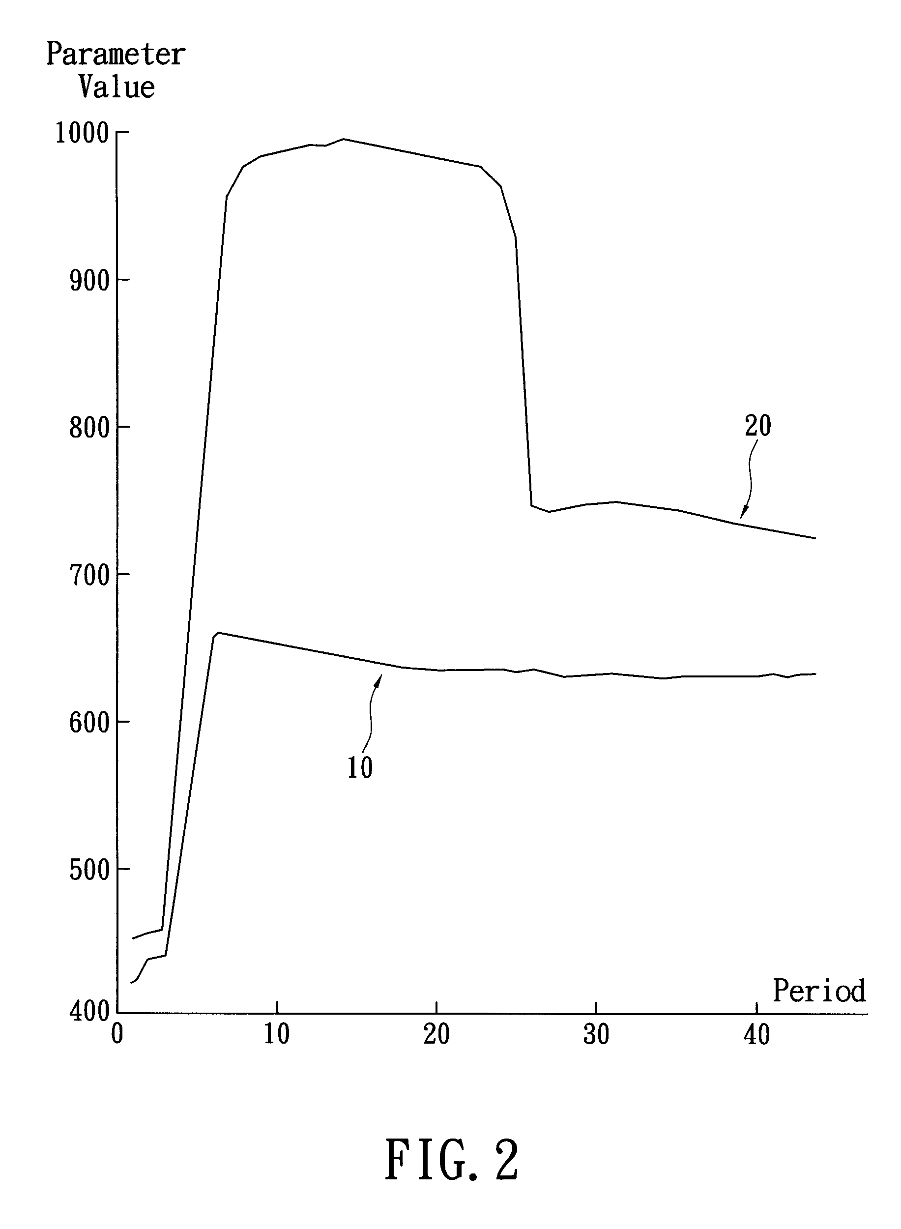
[0026]There exists several tools for semiconductor fabrication, and while the tools are machining on a lot of wafers, the fabrication parameters (e.g voltage values) of such tools may vary along the machining times; for example, a starting voltage value can be zero, then gradually increasing up to a certain value and holds, then subsequently be restored back to zero. Such a variation of fabrication parameter over time can be recorded as a parameter variance curve, and the parameter variance curve can be generated by the Fault Detection and Classification (FDC) system commonly used in the field of semiconductor.

[0027]Each fabrication parameter on a tool has its own normal parameter variance curve, and after machining on a lot of wafers by the tool, suppose the features of the wafers and d...