Method for manufacturing solid-state imaging device

Active Publication Date: 2010-09-16
SONY SEMICON SOLUTIONS CORP
View PDF2 Cites 13 Cited by
  • Summary
  • Abstract
  • Description
  • Claims
  • Application Information

AI Technical Summary

Benefits of technology

[0016]In the method of the embodiment, the offset spacer is provided to the transistor of the logic circuit. Since the offset spacer is formed on the sidewall of the first gate electrode in a state where the photoelectric conversion portion, the pixel transistor region and the floating diffusion region are masked, the regions of the semiconductor substrate where the photoelectric conversion portion, pixel transistors and the floating diffusion portion are to be formed are not damaged to produce a surface defect by etching. Thus, white spots resulting from such a defect can be prevented.
[0017]If the etch back is performed with the floating diffusion region masked with the first insulating layer, the insulating lay

Problems solved by technology

The regions of the silicon substrate where source/drain regions of pixel transistors, particularly of the amplification transistor, are to be formed are damaged by etching for forming offset spacers.
If the substrate is dam

Method used


Image

  • Method for manufacturing solid-state imaging device
  • Method for manufacturing solid-state imaging device
  • Method for manufacturing solid-state imaging device

Examples


Example

First Embodiment

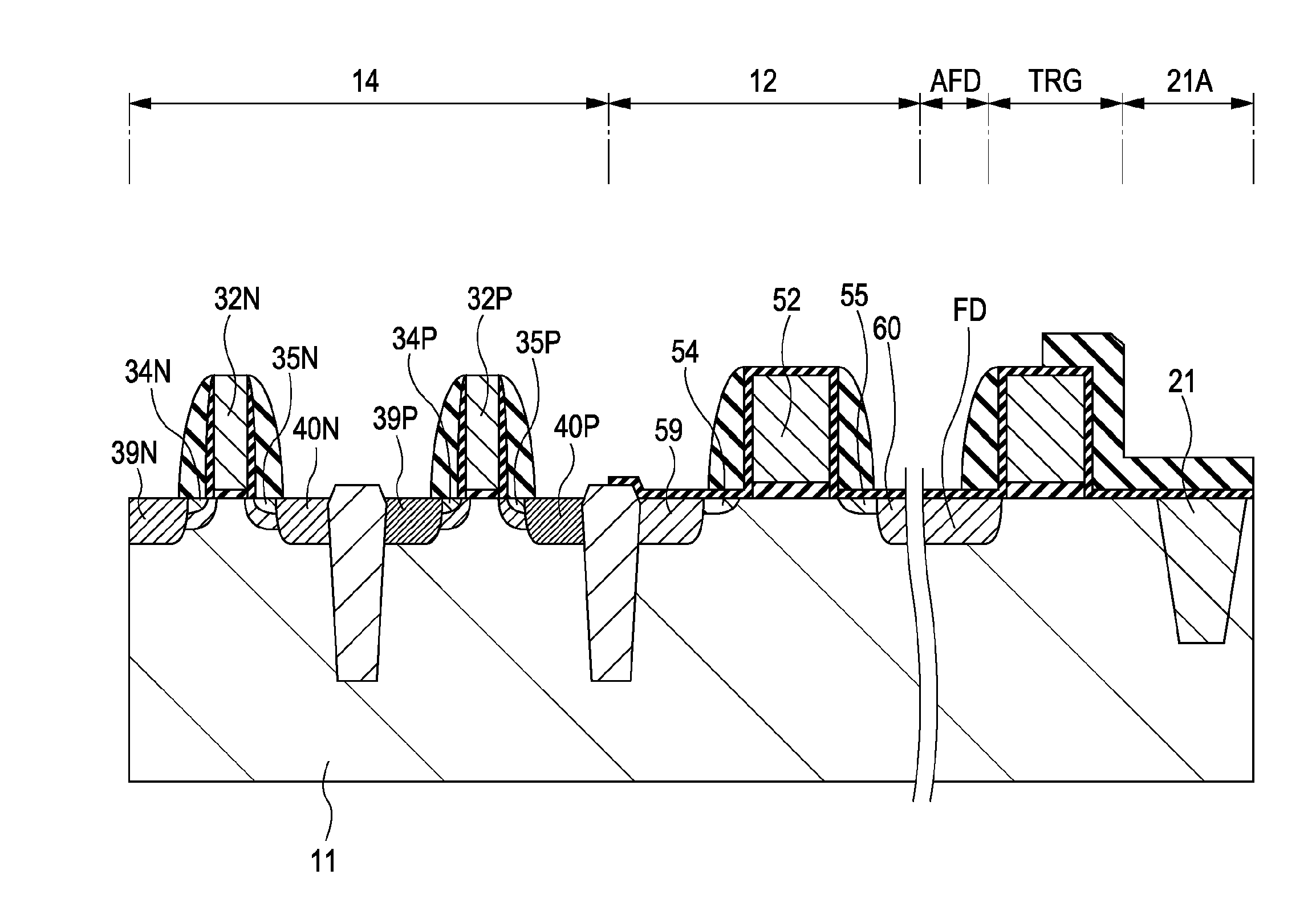
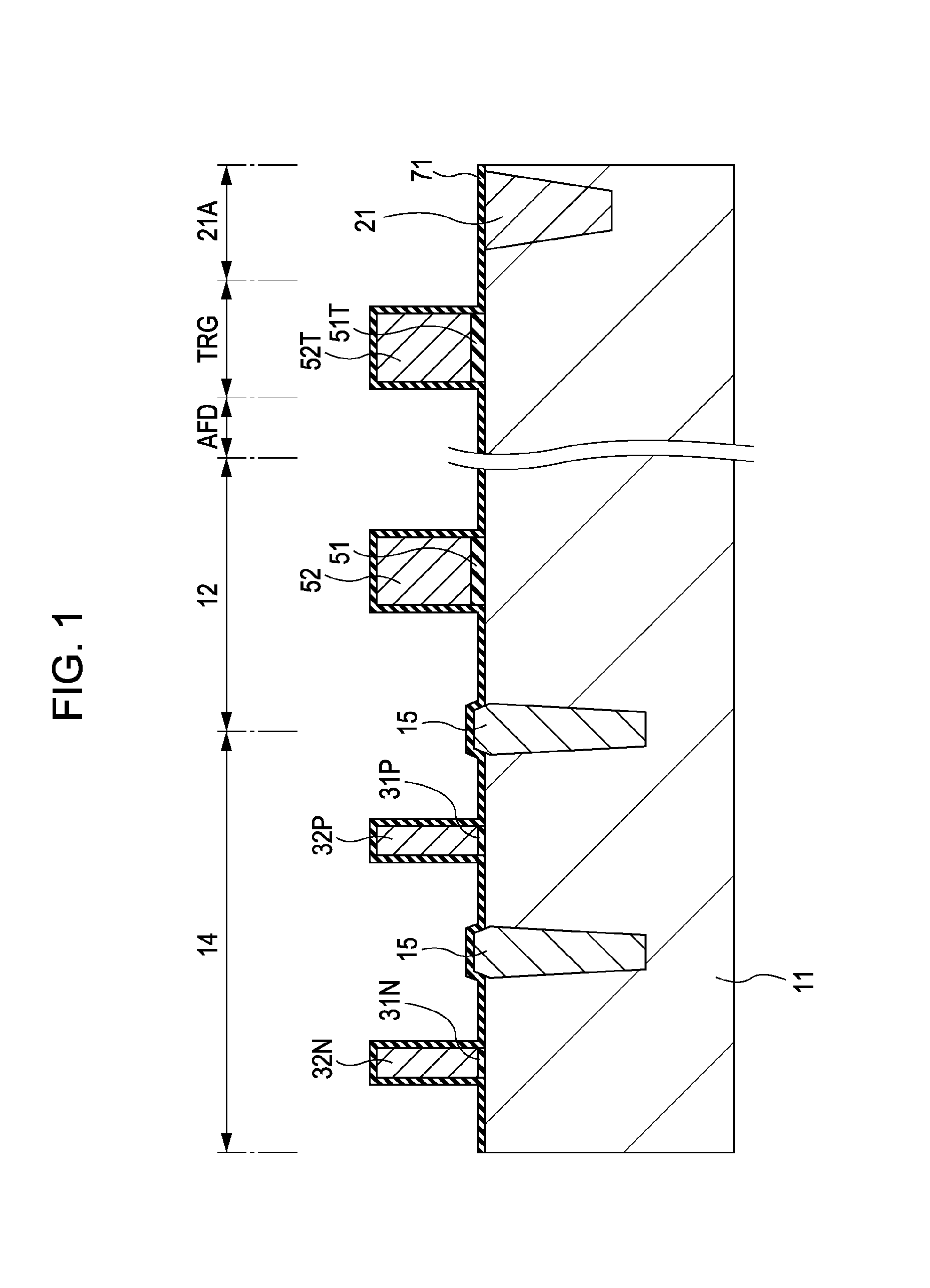
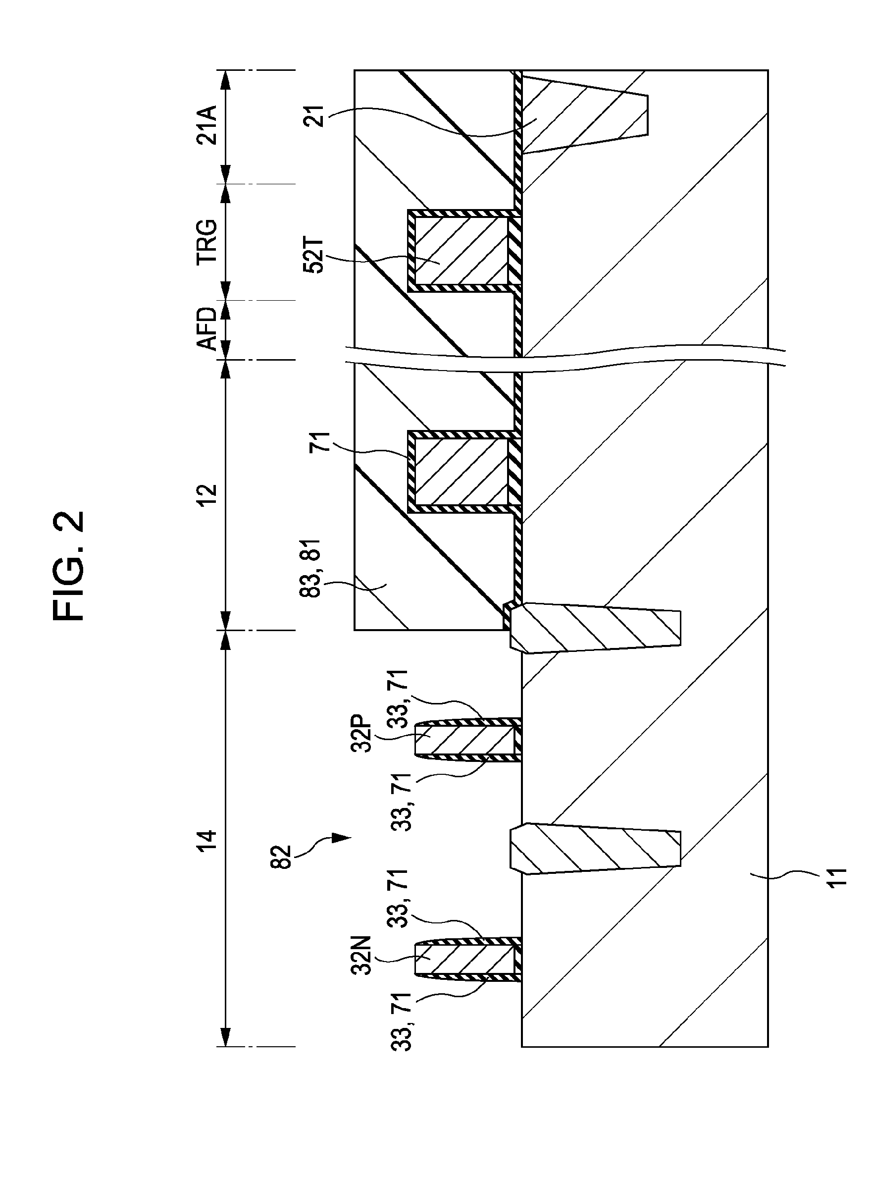
[0034]A method for manufacturing a solid-state imaging device according to an embodiment (first embodiment) of the present invention will now be described with reference to sectional views FIGS. 1 to 7 showing steps of the manufacturing method. The first embodiment illustrates a method for manufacturing a solid-state imaging device including a photoelectric conversion portion, a transfer gate, a floating diffusion portion, a pixel transistor region and a logic circuit region in a semiconductor substrate. The present embodiment features the step of forming an offset spacer on the sidewalls of the gate electrodes of transistors formed in the logic circuit region, and subsequent steps.

[0035]As shown in FIG. 1, element isolation portions 15 (partially shown) are formed in a semiconductor substrate 11 to separate a pixel transistor region 12, a floating diffusion region AFD where a floating diffusion portion is to be formed, and a logic circuit region 14 from each other. ...

Example

Second Embodiment

[0110]A method for manufacturing a solid-state imaging device according to an embodiment (second embodiment) of the present invention will now be described with reference to sectional views FIGS. 9 to 12 showing steps of the manufacturing method.

[0111]As shown in FIG. 9, element isolation portions 15 are formed in a semiconductor substrate 11 to separate a pixel transistor region 12, a floating diffusion region AFD where a floating diffusion portion is to be formed, a logic circuit region 14 and other regions from each other, as described with reference to FIG. 1. The figures show an exemplary structure including two first transistors disposed in the logic circuit region 14, a second transistor disposed in the pixel transistor region 12, a photoelectric conversion portion 21 formed in a photoelectric conversion region 21A, a transfer gate TRG, and the floating diffusion region AFD. The semiconductor substrate 11 may be a silicon substrate. The pixel transistor regio...


PUM


Abstract

A method is provided for manufacturing a solid-state imaging device including a semiconductor substrate having a photoelectric conversion portion, a pixel transistor region and a logic circuit region. The method includes the steps of forming a first gate electrode on the semiconductor substrate with a first gate insulating film therebetween, a second gate electrode in the pixel transistor region on the semiconductor substrate with a second gate insulating film therebetween; forming a first insulating layer to cover the first gate electrode, the second gate electrode, a floating diffusion region where a floating diffusion portion is to be formed, and the photoelectric conversion portion; and forming an offset spacer on a sidewall of the first gate electrode by etch back of the first insulating layer in a state where the photoelectric conversion portion, the pixel transistor region and the floating diffusion region are masked.

Description

BACKGROUND OF THE INVENTION[0001]1. Field of the Invention[0002]The present invention relates to a method for manufacturing a solid-state imaging device.[0003]2. Description of the Related Art[0004]A CMOS image sensor includes a logic circuit whose logical portion includes a transistor having a gate electrode, and the gate length of the gate electrode is most miniaturized.[0005]If the level of transistor miniaturization lies before the 90 nm generation defined by the roadmap for CMOS LSI, in general, desired characteristics can be imparted to the transistor without forming an offset spacer. The offset spacer, which is formed on the sidewall of the gate electrode, is intended to adjust the overlap length (ΔL) of the source / drain extension regions and the gate electrode of the transistor.[0006]In order to install 90 nm generation transistors or later to a solid-state imaging device with a practical ion implantation apparatus or by a practical heat treatment technique, however, ion imp...

Claims


Application Information

Patent Timeline
IPC IPC(8): H01L21/8238
CPCH01L27/14609H01L27/14621H01L27/14627H01L27/146H01L27/14643H01L27/14685H01L27/14689H01L27/1463
Inventor KIMIZUKA, NAOHIKOMATSUMOTO, TAKUJI
Owner SONY SEMICON SOLUTIONS CORP
Why Eureka
Try Eureka