Driver circuit, display device including the driver circuit, and electronic device including the display device
- Summary
- Abstract
- Description
- Claims
- Application Information
AI Technical Summary
Benefits of technology
Problems solved by technology
Method used
Image

Examples
embodiment 1
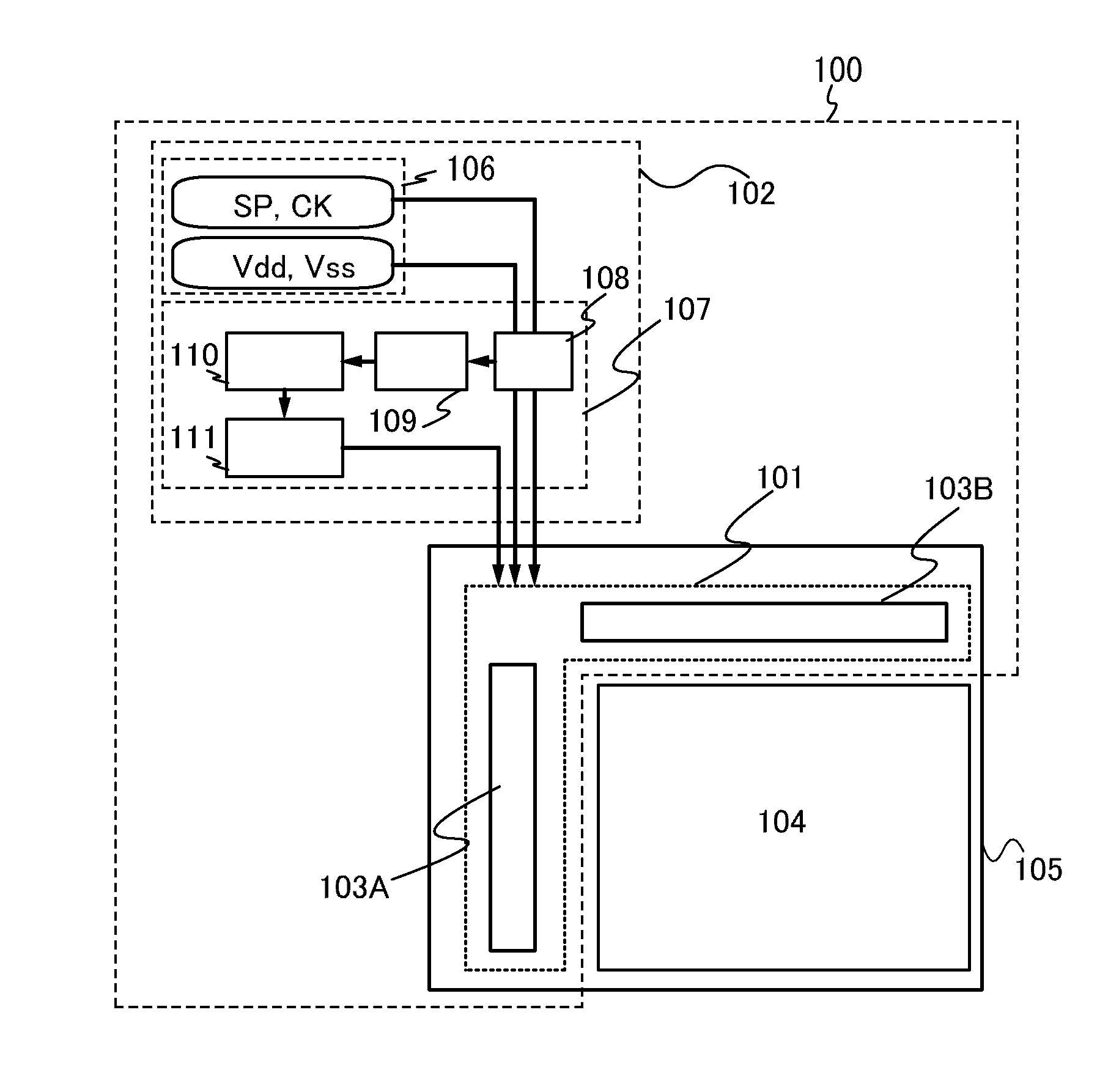
[0034]In this embodiment, a block diagram of circuits near a driver circuit will be described. FIG. 1 illustrates an example of a driver circuit of a display device.
[0035]A driver circuit 100 in this embodiment includes a display portion driver circuit 101 and a control circuit 102.
[0036]The display portion driver circuit 101 includes a gate line driver circuit 103A and a signal line driver circuit 103B, for example. The gate line driver circuit 103A and the signal line driver circuit 103B are each a driver circuit which drives a display portion 104 including a plurality of pixels. The gate line driver circuit 103A, the signal line driver circuit 103B, and the display portion 104 are formed using thin film transistors which are formed over a substrate 105.
[0037]Note that the thin film transistors included in the gate line driver circuit 103A, the signal line driver circuit 103B, and the display portion 104 are unipolar transistors, specifically, n-channel thin film transistors. As a...
embodiment 2
[0081]In this embodiment, the driver circuit described in the above embodiment and a cross-sectional view of a display device including a display portion controlled by the driver circuit will be described with reference to FIG. 5. Further, in this embodiment, an example of a liquid crystal display device will be described as the display device; however, the present invention can be used for another display device including a light-emitting element such as an organic EL element or a driver circuit for an electronic paper including an electrophoretic element. Note that the structure described in the above embodiment can be applied to a different device such as a driver circuit for an optical sensor, in addition to the driver circuit of the display device.
[0082]A liquid crystal display device which is one embodiment of the present invention is illustrated in FIG. 5. In the liquid crystal display device in FIG. 5, a substrate 706 which is provided with a pixel portion including a thin f...
embodiment 3
[0088]In this embodiment, an example in which at least some of driver circuits and a thin film transistor provided in a pixel portion are formed over the same substrate will be described below. Note that the thin film transistor formed over the substrate may be formed as illustrated in the cross-sectional view in Embodiment 2.
[0089]The signal line driver circuit includes a shift register 5601 and a switching circuit 5602. The switching circuit 5602 includes a plurality of switching circuits 5602_1 to 5602_N (N is a natural number). The switching circuits 5602_1 to 5602_N each include a plurality of thin film transistors 5603_1 to 5603—k (k is a natural number). An example where the thin film transistors 5603_1 to 5603—k are n-channel TFTs is described below.
[0090]A connection relation in the signal line driver circuit is described using the switching circuit 5602_1 as an example. First terminals of the thin film transistors 5603_1 to 5603—k are connected to wirings 5604_1 to 5604—k,...
PUM
 Abstract
Description
Claims
Application Information
 - R&D
- Intellectual Property
- Life Sciences
- Materials
- Tech Scout
- Unparalleled Data Quality
- Higher Quality Content
- 60% Fewer Hallucinations
Browse by: Latest US Patents, China's latest patents, Technical Efficacy Thesaurus, Application Domain, Technology Topic, Popular Technical Reports.
© 2025 PatSnap. All rights reserved.Legal|Privacy policy|Modern Slavery Act Transparency Statement|Sitemap|About US| Contact US: help@patsnap.com