On-Chip Logic To Support In-Field Or Post-Tape-Out X-Masking In BIST Designs

a logic and bist technology, applied in the field of selective masking of data, can solve the problems of increasing the number of test vectors, requiring larger and larger amounts of test vector memory, and manufacturing newer integrated circuits requires even more complex manufacturing techniques

Inactive Publication Date: 2010-10-07
MENTOR GRAPHICS CORP
View PDF3 Cites 10 Cited by
  • Summary
  • Abstract
  • Description
  • Claims
  • Application Information

AI Technical Summary

Problems solved by technology

As a result, it requires ever-increasing numbers of test vectors to properly test them, which in turn requires larger and larger amounts of tester vector memory.
Still further, manufacturing newer integrated circuits requires even more complex manufacturing techniques, with the corresponding increase in problems and costs related to the production of integrated circuits.
If these unknown data values (referred to herein as “X values” or “Xs”) are compacted with the relevant data values, then the compacted test signature may not contain enough stable and predictable information to determine if the integrated circuit has one or more of the targeted faults.
With conventional integrated circuits, however, there may be a large number of clock systems using high application frequencies.
As a result, it is often not possible to precalculate all unknowns that may occur due to false path, clock skew, and inaccurate timing models for all of the library elements and layout wires used in the integrated circuit.
While this methodology provides for accurate testing, creating a new layout design with the associated masks for an integrated circuit is very expensive, and increases the time-to-market significantly.

Method used


Image

  • On-Chip Logic To Support In-Field Or Post-Tape-Out X-Masking In BIST Designs
  • On-Chip Logic To Support In-Field Or Post-Tape-Out X-Masking In BIST Designs
  • On-Chip Logic To Support In-Field Or Post-Tape-Out X-Masking In BIST Designs

Examples


Embodiment Construction

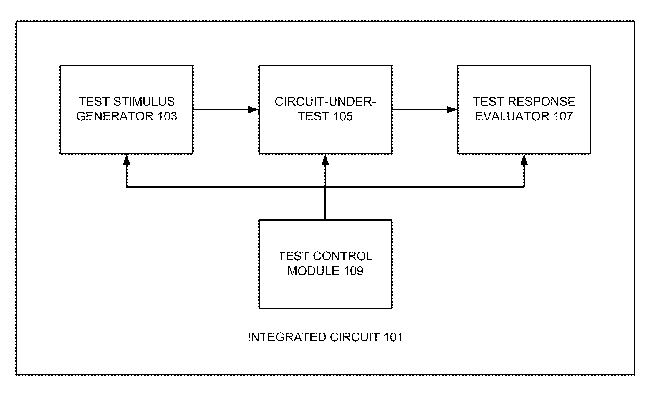
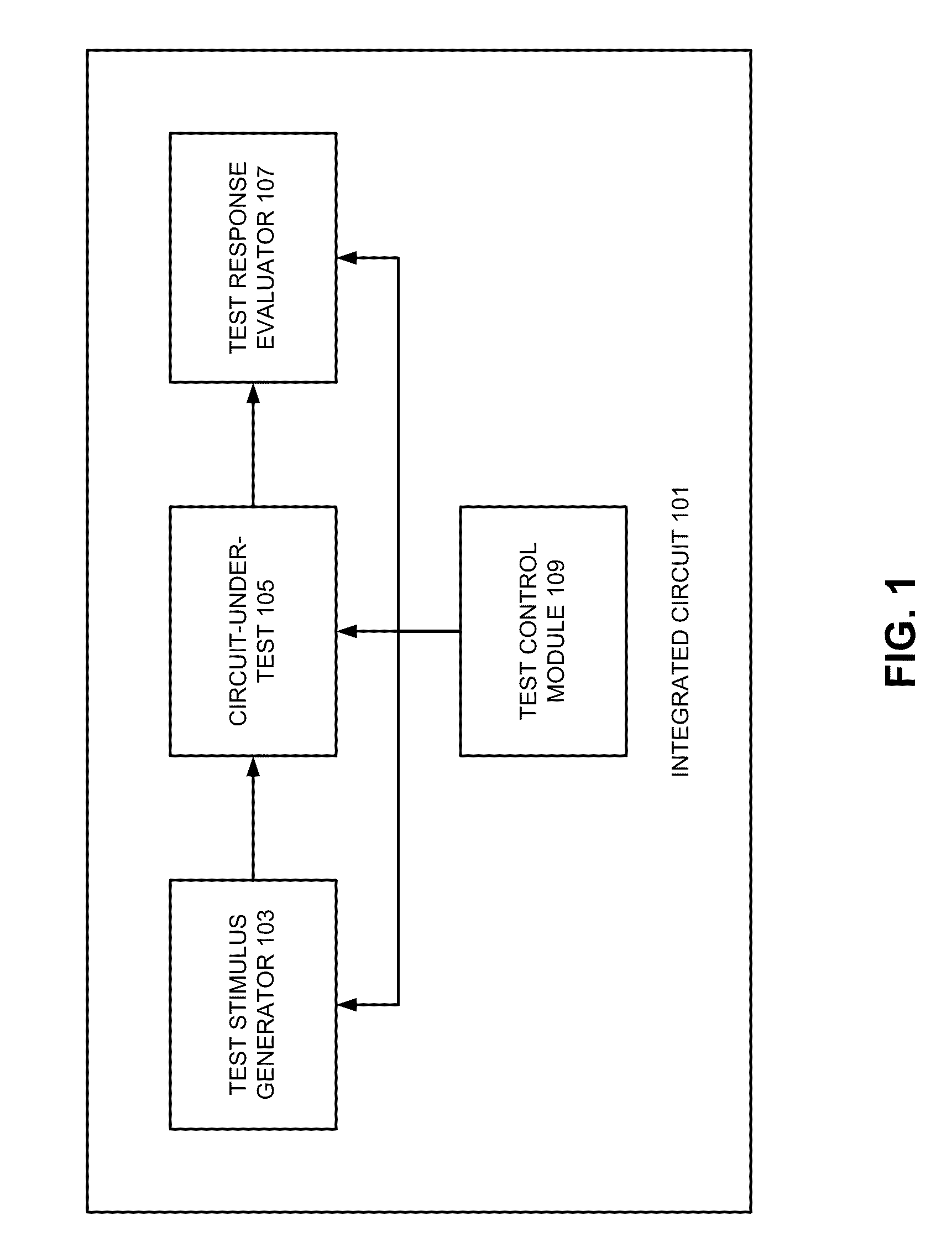
Built-In Self-Test System

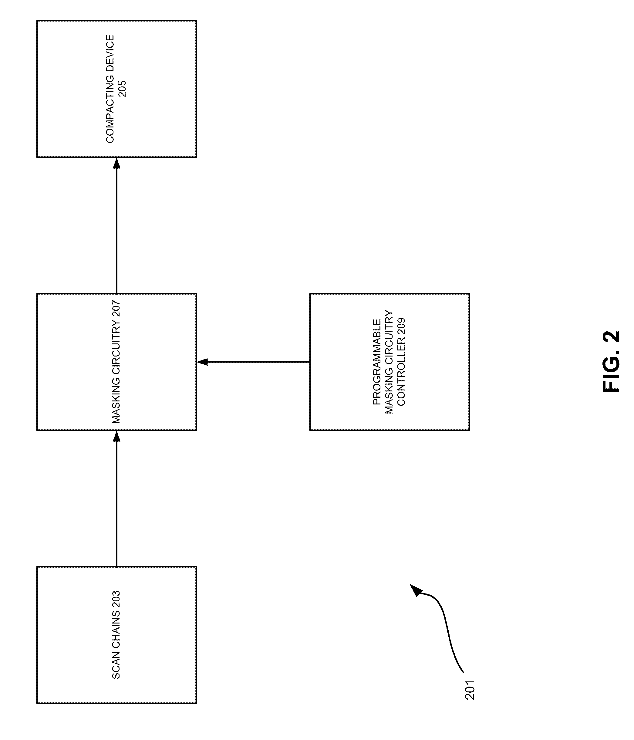
[0013]FIG. 2 illustrates a generic representation of a built-in self-test system that that can be used to perform post-tape-out or in-field masking of unknown test response values according to various implementations of the invention. As seen in this figure, the built-in self-test system 201 includes one or more scan chains 203 and a compacting device 205. The self-test system 201 also includes masking circuitry 207 and a programmable masking circuitry controller 209. With various examples of the invention, the scan chains 203 may operate in a conventional manner. That is, the scan chains 203 operate to apply test vectors to circuitry under test, and then capture the test response values produced by the tested circuitry. The masking circuitry 205 then serves to mask unknown values among the test response values.

[0014]More particularly, the masking circuitry 207 will mask specific unknown values in response to control information provided by the programmable ...


PUM


Abstract

Techniques for masking unknown and irrelevant response values that may be produced by a BIST process. Masking circuitry is provided for selectively masking the response values obtained from a BIST process. The operation of the selective masking circuitry is controlled by a programmable mask circuitry controller that can be programmed after the integrated circuit has been manufactured. A user can analyze an integrated circuit after it has been manufactured to identify irrelevant and unknown data values in a BIST process. After the irrelevant and unknown data values have been identified, the user can program the programmable mask controller to have the selective masking circuitry mask the identified irrelevant and unknown data values.

Description

RELATED APPLICATIONS[0001]This application claims priority to U.S. Provisional Patent Application No. 61 / 117,230, entitled “On-Chip Logic To Support In-Field Or Post-Tape-Out X-Masking In Logic-BIST Designs,” filed on Nov. 23, 2008, and naming Friedrich Hapke et al. as inventors, which application is incorporated entirely herein by reference.FIELD OF THE INVENTION[0002]The present invention is directed to the selective masking of data generated by a scan-chain test of an integrated circuit device. Various implementations of the invention may be particularly useful for allowing a manufacturer to select the data to be masked after the integrated circuit device has been manufactured.BACKGROUND OF THE INVENTION[0003]As integrated circuits continue to develop, they continue to have higher device densities and clocking rates. As a result, it requires ever-increasing numbers of test vectors to properly test them, which in turn requires larger and larger amounts of tester vector memory. Sti...

Claims


Application Information

Patent Timeline
Patent Type & Authority Applications(United States)
IPC IPC(8): G01R31/26
CPCG06F11/27G01R31/318544
Inventor HAPKE, FRIEDRICHWITTKE, MICHAEL
Owner MENTOR GRAPHICS CORP
Why Eureka
Try Eureka