Broadband and wavelength-selective bidirectional 3-way optical splitter

a bidirectional, wavelength-selective technology, applied in the field of bidirectional, 3-way optical splitters, can solve the problems of increasing power consumption of high-performance microprocessors, increasing latency of global on-chip wires, and limiting further clock frequency increases

Active Publication Date: 2010-10-21
ORACLE INT CORP
View PDF5 Cites 23 Cited by
  • Summary
  • Abstract
  • Description
  • Claims
  • Application Information

AI Technical Summary

Benefits of technology

[0032]Another embodiment of the present invention provides an array of chip modules that include one or more instance of the 3-way, bidirectional optical splitter.

Problems solved by technology

Unfortunately, several issues are beginning to constrain further increases in the clock frequency.
In particular, the latency of global on-chip wires is increasing as technological trends reduce their thickness but not their length.
Moreover, as integration densities and clock frequencies continue to increase, the power consumption of high-performance microprocessors also increases.
Consequently, many existing microprocessors consume over 100 W of power, which strains the capabilities of air cooling systems.
In fact, many microprocessors have become power-limited, which means they could be operated at higher clock frequencies at the cost of significant increases in power consumption, and thus, in required cooling.
These design constraints have led designers to change microprocessor designs.
This gap often limits system performance because the microprocessor spends an increasing amount of time waiting for memory accesses instead of executing code.
Given the aforementioned latency problems, it may be difficult to meet these requirements using conventional conductive wires.
Unfortunately, in multi-chip systems, data conflicts on optical signal paths can occur at boundaries between chips.
However, this can significantly increase the number of different types of chips in such a system, with a commensurate impact on the complexity and cost of the multi-chip system.

Method used


Image

  • Broadband and wavelength-selective bidirectional 3-way optical splitter
  • Broadband and wavelength-selective bidirectional 3-way optical splitter
  • Broadband and wavelength-selective bidirectional 3-way optical splitter

Examples


Embodiment Construction

[0072]The following description is presented to enable any person skilled in the art to make and use the invention, and is provided in the context of a particular application and its requirements. Various modifications to the disclosed embodiments will be readily apparent to those skilled in the art, and the general principles defined herein may be applied to other embodiments and applications without departing from the spirit and scope of the present invention. Thus, the present invention is not intended to be limited to the embodiments shown, but is to be accorded the widest scope consistent with the principles and features disclosed herein.

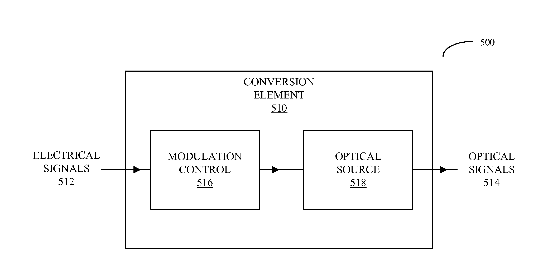
[0073]Embodiments of a bidirectional 3-way optical splitter and a method for 3-way splitting an optical signal are described. This bidirectional 3-way

[0074]optical splitter may include: an optical splitter that has: a first external node, a second external node, a third external node, and a fourth external node. In one mode of operation, the op...


PUM


Abstract

Embodiments of a bidirectional 3-way optical splitter are described. This bidirectional 3-way optical splitter includes an optical splitter having: a first external node, a second external node, a third external node, and a fourth external node. In one mode of operation, the optical splitter may be configured to receive an external input optical signal on the first external node and to provide external output optical signals on the other external nodes. Moreover, in another mode of operation, the optical splitter may be configured to receive the external input optical signal on the third external node and to provide the external output optical signals on the other external nodes.

Description

CROSS REFERENCE TO RELATED APPLICATIONS[0001]This application is related to U.S. patent application Ser. No. “______”, entitled “Optical-Signal-Path Routing in a Multi-Chip System,” filed Dec. ______, 2007; U.S. patent application Ser. No. “11 / 863,815”, entitled “Wavelength-Division Multiplexing for Use in Multi-Chip Systems,” filed Sep. 28, 2007; U.S. patent application Ser. No. “11 / 853,316”, entitled “Multi-Chip Systems with Optical Bypass,” filed Sep. 11, 2007; U.S. patent application Ser. No. 11 / 728,845, entitled “Multi-Chip Systems Using On-Chip Photonics,” filed Mar. 26, 2007; U.S. patent application Ser. No. 11 / 728,844, entitled “Low-Latency Switch Using Optical and Electrical Proximity Communication,” filed Mar. 26, 2007; U.S. patent application Ser. No. 11 / 728,843, entitled “Transparent Switch Using Optical and Electrical Proximity Communication,” filed Mar. 26, 2007; U.S. patent application Ser. No. 11 / 515,085, entitled “Resonator System for Optical Proximity Communication...

Claims


Application Information

Patent Timeline
Patent Type & Authority Applications(United States)
IPC IPC(8): H04J14/00
CPCG02B6/2804G02B6/29343G02B6/29352H04Q2213/13322G02B2006/1215H04J14/0212H04Q2213/1301G02B6/43
Inventor ZHENG, XUEHZEO'KRAFKA, BRIAN W.KRISHNAMOORTHY, ASHOK V.CUNNINGHAM, JOHN E.
Owner ORACLE INT CORP
Why Eureka
Try Eureka