Solid-state imaging apparatus

a solid-state imaging and imaging apparatus technology, applied in the direction of television systems, radio-controlled devices, instruments, etc., can solve the problems of increasing the width between the holding units of each pixel column, increasing the interval between the pixels, and severe limitations in the arrangement of the a/d converter provided for each column of pixels, so as to reduce the pitch of the pixel arrangement

Active Publication Date: 2010-11-18
CANON KK
View PDF13 Cites 23 Cited by
  • Summary
  • Abstract
  • Description
  • Claims
  • Application Information

AI Technical Summary

Benefits of technology

[0011]An object of the present invention is to provide a solid-state imaging apparatus that can reduce a pixel arrangement pitch.
[0013]The pixel arrangement pitch in the direction along rows of the two-dimensional array of pixels is easily reduced.

Problems solved by technology

Meanwhile, accompanying the miniaturization of pixels, there are severe limitations with respect to the arrangement of the A / D converters provided for each column of pixels.
H05-48460, there is the problem that because the circuit diagram illustrates a circuit in which respective holding units for each bit are arranged in parallel in the direction along a row, the interval between the pixels increases when elements are disposed as shown in the circuit diagram.
However, neither Japanese Patent Application Laid-Open No.
H05-48460, there is the problem that the width between the holding units of each pixel column increases.

Method used


Image

  • Solid-state imaging apparatus
  • Solid-state imaging apparatus
  • Solid-state imaging apparatus

Examples


first embodiment

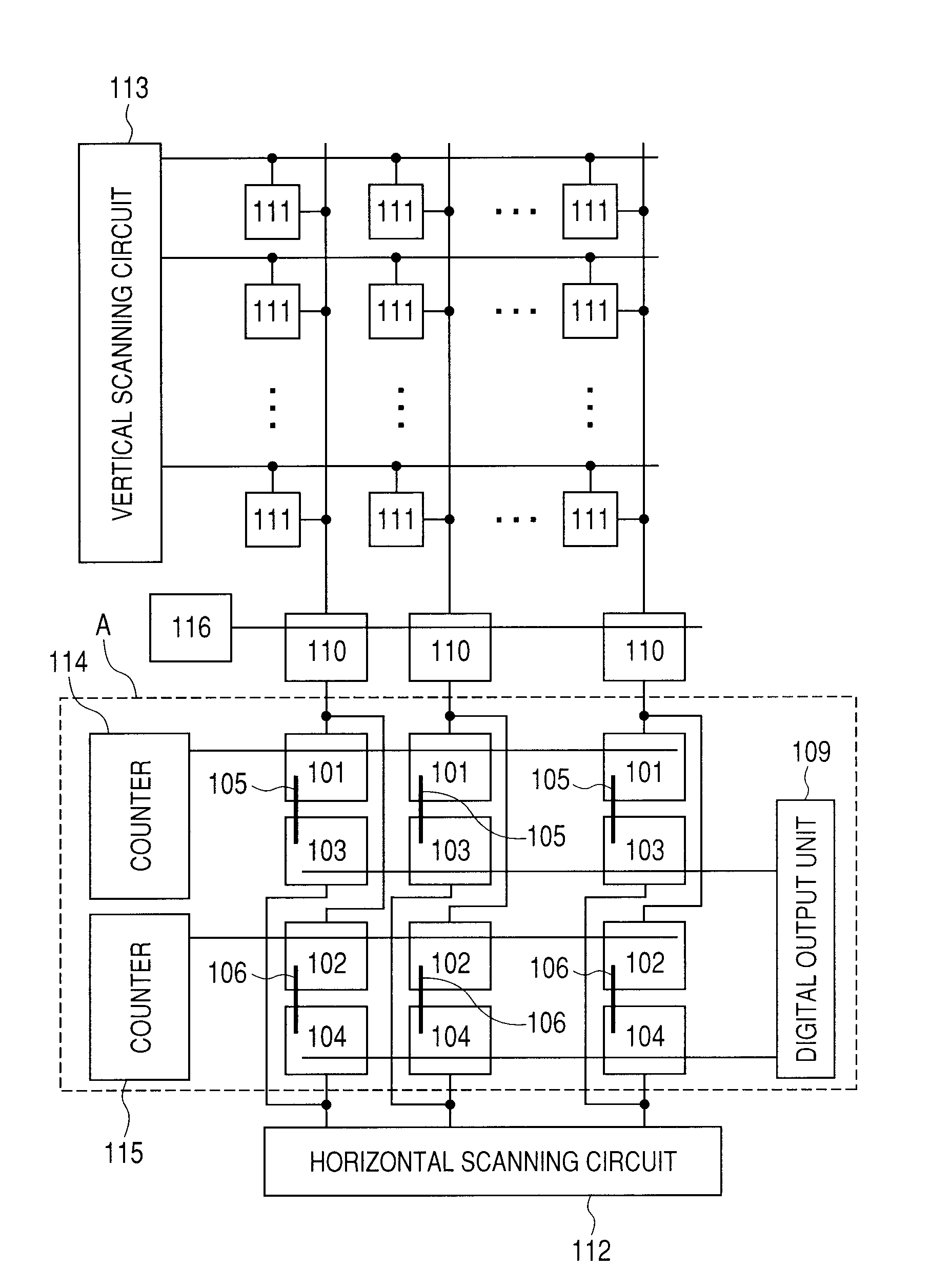
[0023]FIG. 1 is an overall configuration diagram of a solid-state imaging apparatus according to a first embodiment of the present invention. A plurality of pixels 111 having photoelectric conversion elements are arranged in a two-dimensional array. The photoelectric conversion elements are, for example, photodiodes that generate image signals by photoelectric conversion. A vertical scanning circuit 113 selects the pixels 111 row by row, and reads out analog signals generated in the selected pixels 111. The read-out signals are input to an A / D (analog / digital) converter that is provided for each column of pixels 111. The A / D converter converts the analog signals into digital signals. A comparator 110 included in the A / D converter compares the magnitude of a read-out signal and a comparison signal. Counters 114 and 115 are commonly provided for each column of pixels 111 to count a digital signal value. A first holding unit 101 is provided for each column of pixels 111, and holds a hi...

second embodiment

[0029]FIG. 3 is a layout diagram illustrating a second embodiment of the region A in the solid-state imaging apparatus in FIG. 1. Components in FIG. 3 that are the same as those in FIG. 1 and FIG. 2 are denoted by the same reference numbers. Holding unit groups formed by arranging the first holding units 101 and third holding units 103 closely to each other in pairs, respectively, in the row direction, and holding unit groups formed by arranging the second holding units 102 and fourth holding units 104 closely to each other in pairs, respectively, in the row direction, are arranged in the column direction. The arrangement illustrated in FIG. 3 enables the length in the column-wise direction to be reduced with respect to the configuration illustrated in FIG. 2.

[0030]Digital data from the first counter 114 is supplied to the first holding unit 101 through data line 107. Digital data from the second counter 115 is supplied to the second holding unit group 102 through data line 107. The...

third embodiment

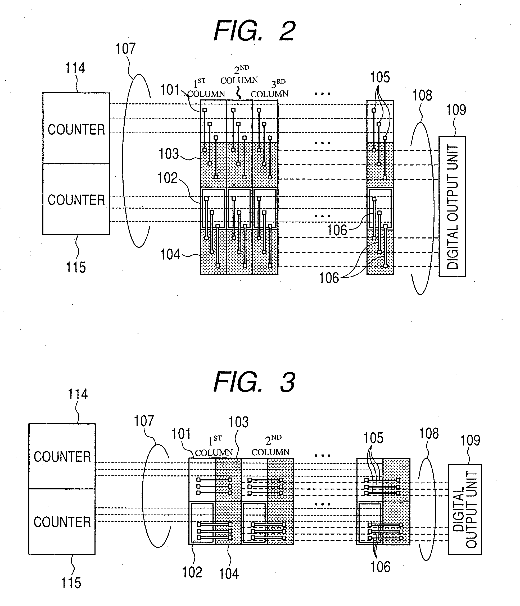
[0031]FIG. 4 is a layout diagram illustrating a third embodiment of the region A in FIG. 1. Components in FIG. 4 that are the same as those in FIG. 1 and FIG. 2 are denoted by the same reference numbers. The difference between the present embodiment and the first embodiment is described hereafter. Similarly to FIG. 1, the first holding units 101 and the third holding units 103 are arranged closely to each other in the order of holding unit 101—holding unit 103 from the higher order bits. Conversely to the arrangement illustrated in FIG. 1, the second holding units 102 and the fourth holding units 104 are arranged closely to each other in the order of holding unit 104—holding unit 102 from the higher order bits. By adopting this arrangement, it is possible to concentrate the line of output lines 108, thus facilitating the arrangement. Further, it is possible to reduce the required area when implementing a measure to counter the effects of cross talk from output lines 108 to other ele...


PUM


Abstract

A solid-state imaging apparatus includes a plurality of pixels for converting analog image signals from the pixels into digital signals including a higher digit bit and a lower digit bit in time series. The A / D converter includes a first holding unit for holding the higher digit bit of the digital signal, a second holding unit for holding the lower digit bit of the digital signal, a third holding unit for holding the digital signal from the first holding unit, and a fourth holding unit for holding the digital signal from the second holding unit. A first pair including the first and third holding units, and a second pair including the second and fourth holding units are arranged in a direction along the column of the two-dimensional array of pixels.

Description

BACKGROUND OF THE INVENTION[0001]1. Field of the Invention[0002]The present invention relates to a solid-state imaging apparatus.[0003]2. Description of the Related Art[0004]In recent years, the numbers of pixels of solid-state imaging apparatuses are being increased to enhance the quality of captured images in image input apparatuses such as digital still cameras and digital video cameras. Image input apparatuses are also available which reduce costs by mounting an A / D converter in a solid-state imaging apparatus to realize a digital output.[0005]One example of an A / D conversion system mounted in a solid-state imaging apparatus is a column A / D conversion system (for example, see Japanese Patent Application Laid-Open No. H05-48460).[0006]A column A / D conversion system includes an A / D converter for each column of pixels, and operates the A / D converters in parallel. Hence, the column A / D conversion system can enhance the readout speed of a solid-state imaging apparatus. Meanwhile, acc...

Claims


Application Information

Patent Timeline
Patent Type & Authority Applications(United States)
IPC IPC(8): H04N5/335H01L27/146H03M1/12H03M1/56H04N5/369H04N5/374H04N5/378
CPCH03M1/123H04N5/378H04N5/374H03M1/14H04N25/76H04N25/75
Inventor SHIBATA, MASANORIKOBAYASHI, MASAHIRO
Owner CANON KK
Why Eureka
Try Eureka