This helps you quickly interpret patents by identifying the three key elements:
Problems solved by technology
Method used
Benefits of technology
Benefits of technology
[0013] An object of the present invention is to prevent optical crosstalk in a rear-illuminated-type photodiode array that is to be used as a receiving section for optical communication or a two-dimensionally arranged optical sensor.
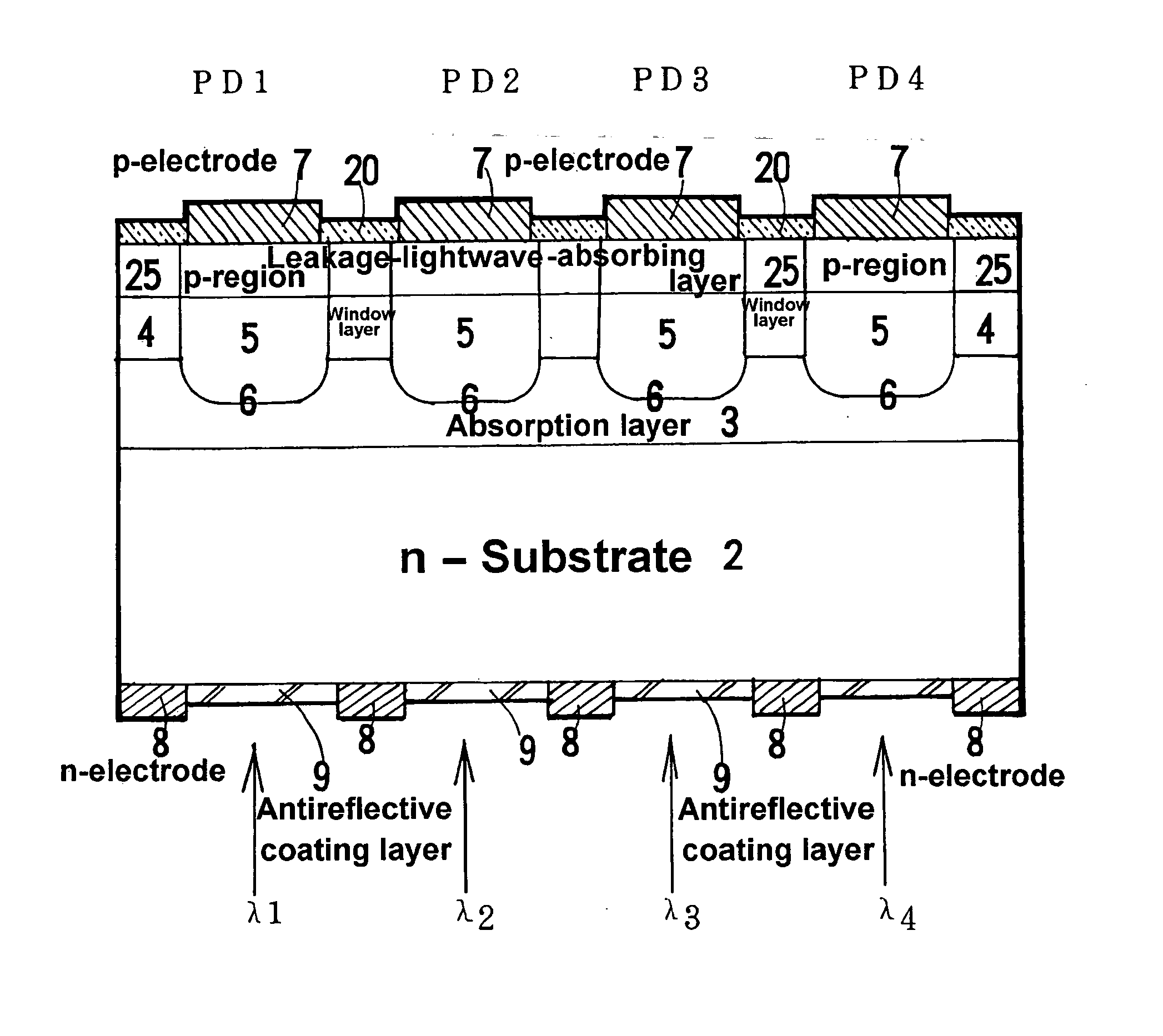
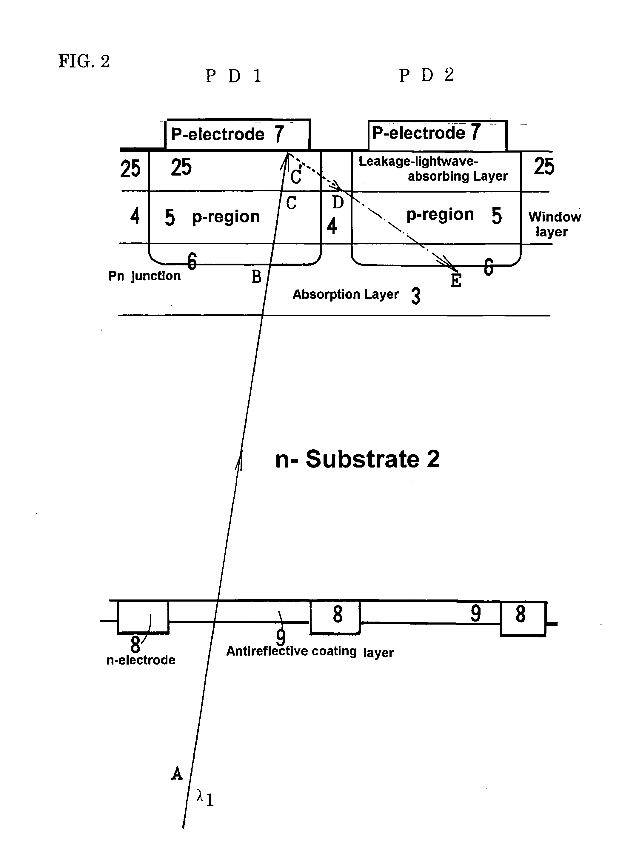
[0030] According to the present invention, in a rear-illuminated-type photodiode array, a leakage-lightwave-absorbing layer is provided between the front-face electrode and the absorption layer, as an innovation. Consequently, even when a lightwave having entered from the rear side is reflected irregularly from the front-face electrode, the lightwave is entirely absorbed by the leakage-lightwave-absorbing layer without entering a neighboring photodiode. As a result, the photodiode array can reduce optical crosstalk between neighboring photodiodes. This enables the achievement of a photodiode array having high sensitivity with less noise. Because the optical crosstalk between neighboring photodiode units is reduced, the spacing between photodiode units can be reduced more than ever before. Thus, the size of the photodiode array can be reduced further. In the case of a two- or one-dimensionally arranged sensor, the arranging pitch of the photodiodes can be reduced, so that the spatial resolution can be increased. When the photodiode array is used for a sensor in an image pickupsystem, the resolution can be increased.
Problems solved by technology
However, in the case of independent photodiodes, it is difficult to reduce the pitch to such a small value.
Because photodiode units having a comparable function are arranged with a small pitch, electrical crosstalk poses a problem.
However, not all of an incoming lightwave is absorbed in the absorption layer.
In other words, a lightwave having entered a photodiode unit causes a noise to a neighboring photodiode unit.
Method used
Image
Click on the blue label to locate the original text in one second.
Reading with bidirectional positioning of images and text.
[0063] The method of producing a rear-illuminated-type photodiode array of the present invention shown in FIG. 3 is explained below. The following layers were epitaxially grown by the metalorganic vapor phase epitaxial method (MOVPE method) in the following order on an n-type InP substrate 2 that had a thickness of 350 μm, that was doped with sulfur, and that had a carrier concentration of n=3×1018 cm−3:
[0064] an n-type InP buffer layer 30 (thickness: 2 μm, undoped, and carrier concentration: n=1×1015 cm−3);
[0065] an n-type InGaAs absorption layer 3 (thickness: 4 μm, undoped, carrier concentration: n=1×1015 cm−3, and lattice-matched with the InP);
[0066] an n-type InP window layer 4 (thickness: 1.5 μm, undoped, and carrier concentration: n=1×1015 cm−3); and
[0067] an n-type InGaAs leakage-lightwave-absorbing layer 25 (thickness: 3 μm, undoped, and carrier concentration: n=1×1015 cm−3).
[0068] Triethylgallium (TEG), trimethy...
example 2
Two-Dimensionally Arranged Photodiode Array (M×N: FIGS. 4 and 5)
[0073] The present invention can also be applied to a rear-illuminated-type two-dimensionally arranged photodiode array. FIG. 4 shows a partial plan view of it, and FIG. 5 shows a partial cross-sectional view of it. This array is formed by arranging photodiode units, “M×N” in number, on one chip. When viewed from above, a p-region 5, a p-electrode 7, and a bump 40 are concentrically placed to form a unit and a multitude of units are arranged in rows and columns like “islands” in a “sea” of the leakage-lightwave-absorbing layer 25. Actually, the top surface is covered with an antireflective coating and the p-electrodes 7 complementarily. The bumps 40 are made of a low-melting-point alloy formed by vapor deposition, plating, or printing and are to be used for soldering. They are provided to flip-chip-connect the array with an IC chip (such as one having amplifying circuits) provided with electrodes placed with the same t...
example 3
A Photodiode Array Having an n-electrode Placed on a Substrate or Buffer Layer (FIG. 6)
[0076] Examples 1 and 2 show an array in which an n-electrode is provided at the rear side of the substrate. The present invention can also be applied to a photodiode array in which an n-electrode is provided on a portion of a substrate or buffer layer that is exposed by etching a part of the layers epitaxially grown on the substrate. FIG. 6 shows a partial cross-sectional view of the photodiode array. In this case, the photodiode units may be arranged one- or two-dimensionally. The photodiode array is provided with a buffer layer 30, an absorption layer 3, a window layer 4, and a leakage-lightwave-absorbing layer 25 all grown epitaxially on the n-type substrate. Individual p-electrodes 7 are provided on individual p-regions 5. Part of the leakage-lightwave-absorbing layer 25, the window layer 4, and the absorption layer 3 are removed by etching. An n-electrode 8 is placed on the exposed portion ...
PUM
Abstract
A rear-illuminated-type photodiode array has (a) a first-electroconductive-type semiconductor substrate, (b) a first-electroconductive-type electrode that is placed at the rear side of the semiconductor substrate and has openings arranged one- or two-dimensionally, (c) an antireflective coating provided at each of the openings of the first-electroconductive-type electrode, (d) a first-electroconductive-type absorption layer formed at the front-face side of the substrate, (e) a leakage-lightwave-absorbing layer that is provided on the absorption layer and has an absorption edgewavelength longer than that of the absorption layer, (f) a plurality of second-electroconductive-type regions that are formed so as to penetrate through the leakage-lightwave-absorbing layer from the top surface and extend into the absorption layer to a certain extent and are arranged one- or two-dimensionally at the positions coinciding with those of the antireflective coatings at the opposite side, and (g) a second-electroconductive-type electrode provided on the top surface of each of the second-electroconductive-type regions.
Description
BACKGROUND OF THE INVENTION [0001] 1. Field of the Invention [0002] The present invention relates to a rear-illuminated-type photodiode array that can be used as a receiving section for optical communication or a two-dimensionally arranged optical sensor. [0003] 2. Description of the Background Art [0004] The field of optical communication has been achieving widespread adoption of the wavelength division multiplexing (WDM) technology, which enables the transmission and reception of a plurality of optical signals having different wavelengths through a single optical fiber. After the separation of the wavelength-multiplexed optical signals having traveled over a single optical fiber, in order to receive individual optical signals having a different wavelength, a group of independent photodiodes or a photodiode array is used. Because the diameter of the cladding of a single-mode optical fiber is 125 μm, it is desirable that the photodiodes be arranged with a pitch of 125 μm. However, i...
Claims
Application Information
Patent Timeline
Application Date:The date an application was filed.
Publication Date:The date a patent or application was officially published.
First Publication Date:The earliest publication date of a patent with the same application number.
Issue Date:Publication date of the patent grant document.
PCT Entry Date:The Entry date of PCT National Phase.
Estimated Expiry Date:The statutory expiry date of a patent right according to the Patent Law, and it is the longest term of protection that the patent right can achieve without the termination of the patent right due to other reasons(Term extension factor has been taken into account ).
Invalid Date:Actual expiry date is based on effective date or publication date of legal transaction data of invalid patent.

