Semiconductor recording apparatus and semiconductor recording system

a recording apparatus and semiconductor technology, applied in the field of semiconductor recording systems, can solve the problems of increasing the probability of writing errors and the inability to perform sequential recording of moving images, and achieve the effect of reducing the time required for the operation and rewriting the number of errors

Active Publication Date: 2010-11-18
PANASONIC CORP
View PDF9 Cites 0 Cited by
  • Summary
  • Abstract
  • Description
  • Claims
  • Application Information

AI Technical Summary

Benefits of technology

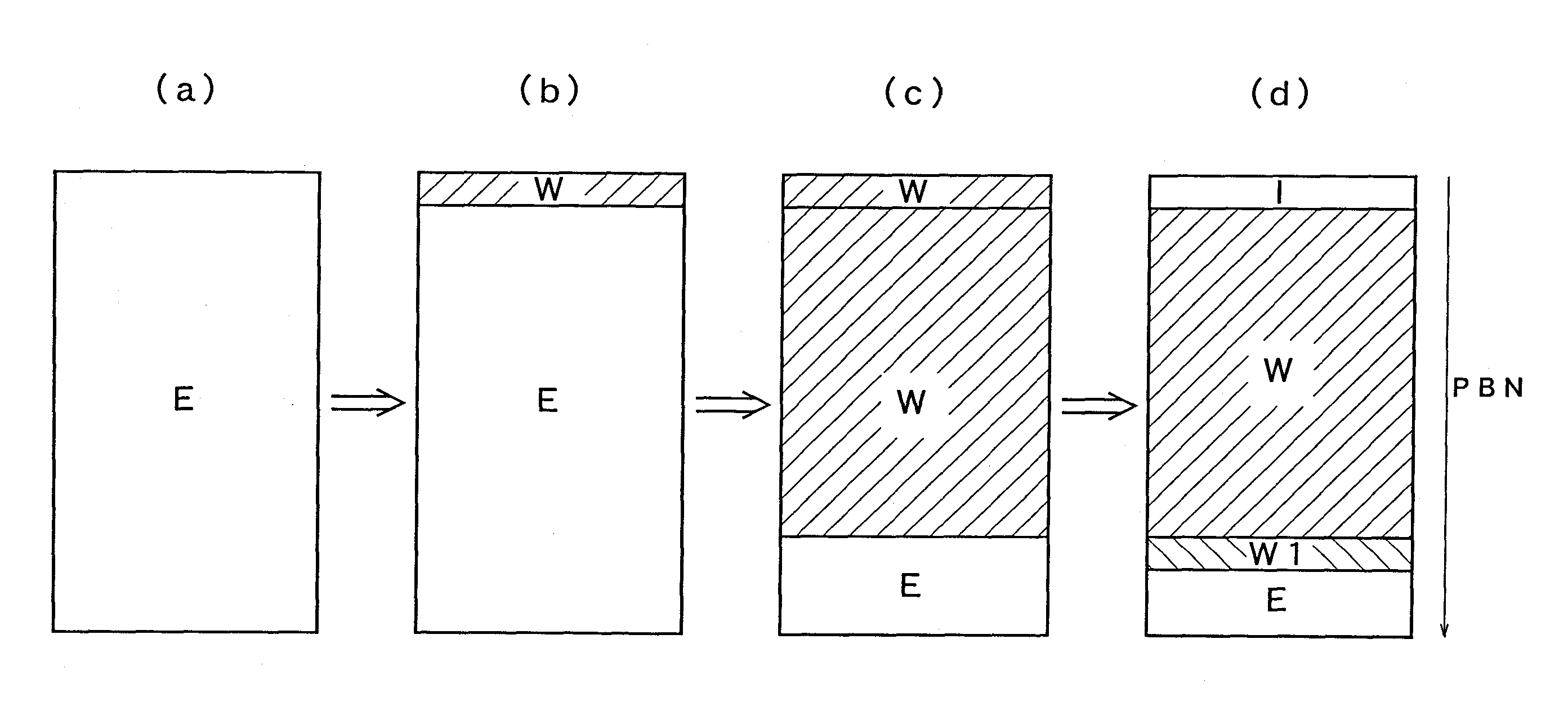
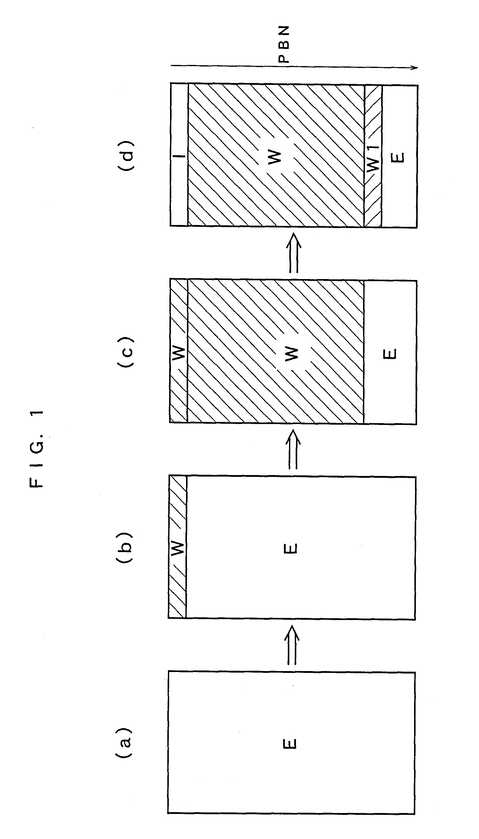
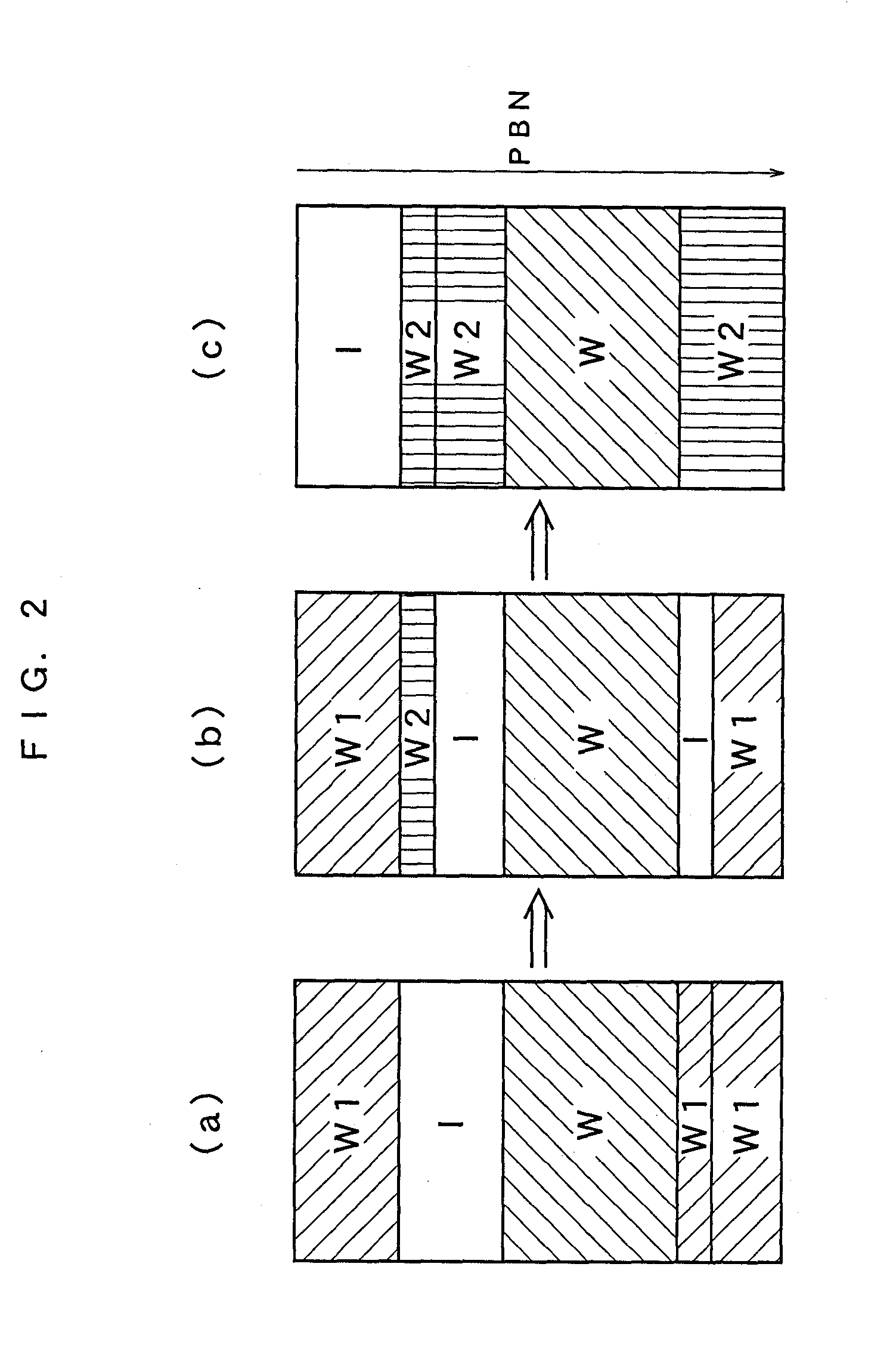
[0031]According to the semiconductor recording apparatus of the present invention, a correlation between a logical address and a physical address can be brought out into the open at the time of logical formatting. Therefore, for example, even if a task involving logical formatting and recording up to a certain extent within capacity is repeated after full-capacity recording, it never occurs that rewrite process is concentrated on part of physical blocks. This makes it possible to render physical blocks of a semiconductor memory uniform in terms of the number of rewrites.
[0032]Moreover, rewrite-number errors that arise in the case of determining the number of rewrites in the conventional semiconductor apparatus disclosed in Patent Document 2 can be significantly reduced.
[0033]Further, according to the present invention, in performing logical formatting, the same effects as achieved in physical formatting to erase all blocks can be achieved, yet the time required for the operation is shorter than that in physical formatting.

Problems solved by technology

When the number of rewrites exceeds 10,000, the probability of writing error occurrence is increased.
This leads to the problem of inability to perform sequential recording of moving images.

Method used


Image

  • Semiconductor recording apparatus and semiconductor recording system
  • Semiconductor recording apparatus and semiconductor recording system
  • Semiconductor recording apparatus and semiconductor recording system

Examples


Embodiment Construction

[0062]In FIG. 3, there is shown a configuration diagram of a semiconductor recording system in accordance with an embodiment of the present invention. In FIG. 3, for example, a semiconductor recording apparatus 100 is built as a memory card, and is connected to a host device 200 to stand ready for use. The semiconductor recording apparatus 100 is composed of a memory controller 110 for exercising data writing-reading control over a flash memory and a flash memory 120 which is a nonvolatile memory.

[0063]The memory controller 110 includes an external interface 111, a command analyzing section 112, a block management section 114, a logical-to-physical conversion table 115, an invalid block management table 116, a logical-to-physical conversion table initializing section 117, and a flash control section 118.

[0064]Next, the memory controller 110 will be described in detail. The external interface 111 is an interface which receives a command from the host device 200 and effects data trans...


PUM


Abstract

A semiconductor recording apparatus includes a logical-to-physical conversion table 115 showing correspondence between a physical address of said semiconductor memory and a logical address and writes the table to a flash memory 120. On receiving a write command issued from a host device 200, a block management section 114 selects a physical block with reference to said logical-to-physical conversion table, and updates said logical-to-physical conversion table. A logical-to-physical conversion table initializing section 117 updates a physical address corresponding to each logical address of the logical-to-physical conversion table into an invalid address. Accordingly the apparatus can render the number of rewrites of physical blocks uniform irrespective of writing conditions.

Description

TECHNICAL FIELD[0001]The present invention relates to a semiconductor recording apparatus such as a memory card and a semiconductor recording system, and more particularly to technologies for rendering physical blocks of a semiconductor memory uniform in terms of the number of times for rewrite process.BACKGROUND ART[0002]Heretofore semiconductor recording equipment such as a SD (Secure Digital) card that is a card-type recording medium having a built-in flash memory has a ultra-compact and ultra-thin form and has been widely used to record data including images in digital cameras, portables, and so forth because of its handleability.[0003]A flash memory incorporated in semiconductor recording equipment is a memory capable of data erasing and rewriting by blocks of a predetermined size, and there is a limitation on the number of rewrites. A multi-level flash memory is designed to allow approximately 10,000 rewrites for each physical block. When the number of rewrites exceeds 10,000,...

Claims


Application Information

Patent Timeline
Patent Type & Authority Applications(United States)
IPC IPC(8): G06F12/10G06F12/00G06F12/02
CPCG06F12/0246G11C8/06G06F2212/7201
Inventor OOTSUKA, TAKESHI
Owner PANASONIC CORP
Why Eureka
Try Eureka