OLED lighting devices including electrodes with magnetic material

a technology of magnetic material and lighting device, which is applied in the direction of lighting support device, discharge tube luminescnet screen, lighting arts, etc., can solve the problems of reducing the value of the large illumination area of the unpackaged device, the disadvantages of the current electrical interconnection technology, and the mounting and electrical interconnection technology of such devices

Active Publication Date: 2010-11-25
BOE TECH GRP CO LTD
View PDF14 Cites 44 Cited by
  • Summary
  • Abstract
  • Description
  • Claims
  • Application Information

AI Technical Summary

Problems solved by technology

One deficiency in the state of the art lies in the mounting and electrical interconnect technologies for such devices.
Although thin film solid state lighting devices can be made thin, large-area, and optionally flexible, these advantages are currently lost to a substantial degree due to size, bulkiness, and rigidity of existing mounting and electrical power input structures.
A disadvantage is that the lateral area occupied by the edge electrodes and corresponding mating structures reduces the light emission area of the packaged lighting device, thus reducing the value of the large illumination area of the unpackaged device.
For OLED devices which are susceptible to damage from ambient moisture or oxygen, the edge connectors also compromise the hermetic seal at the edges of the confining glass or plastic plates or films.
Although the on-board inductive coil is described as “planar”, the addition of these on-board component inherently introduces additional complexity, bulk, and thickness to the OLED device.
The on-board mounting clamps, screws, or magnets contribute still further to the complexity, bulk, and thickness of the OLED lighting devices.

Method used


Image

  • OLED lighting devices including electrodes with magnetic material
  • OLED lighting devices including electrodes with magnetic material
  • OLED lighting devices including electrodes with magnetic material

Examples


Embodiment Construction

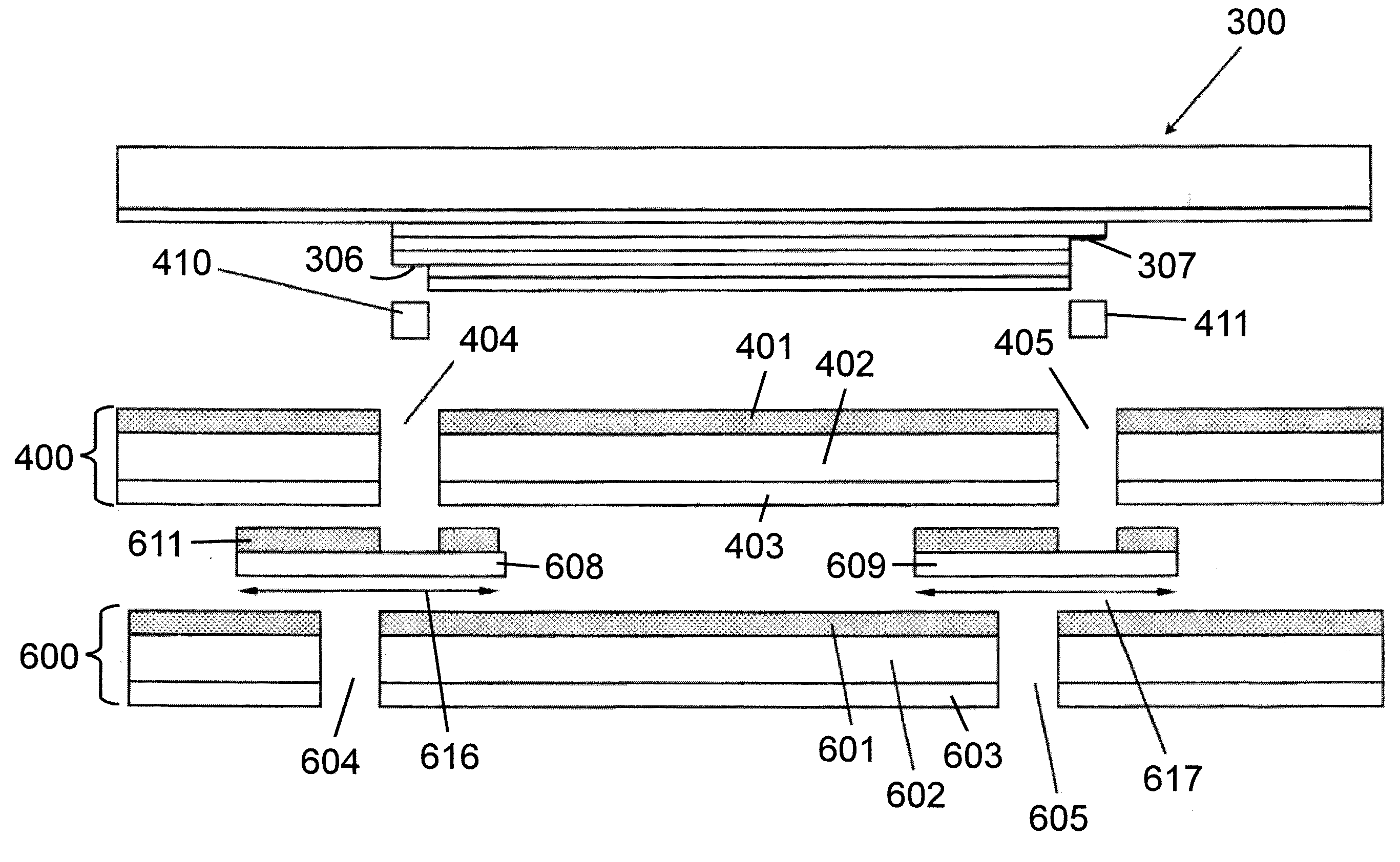
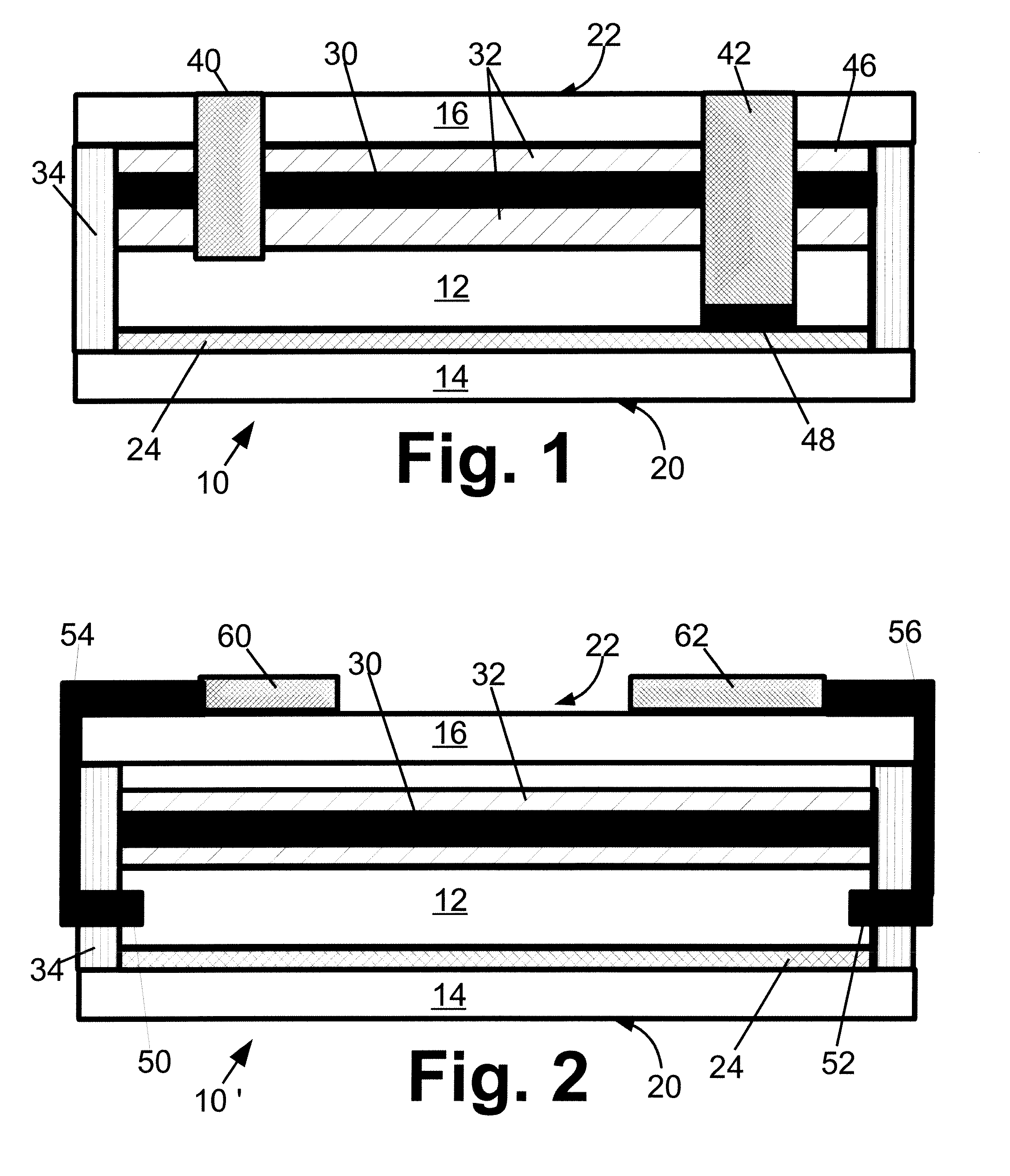
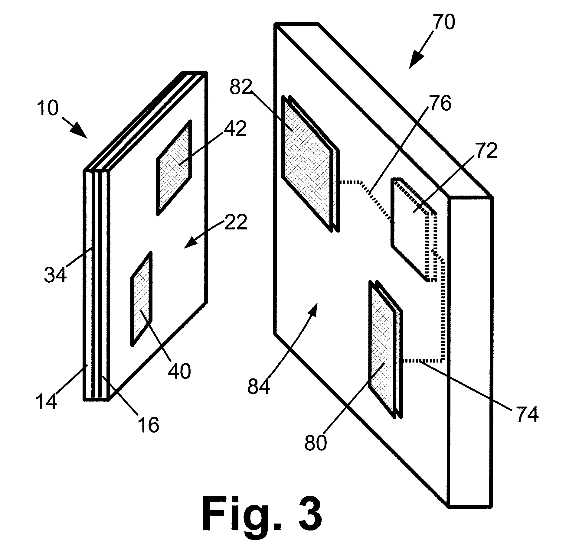
[0015]With reference to FIG. 1, a thin film solid state lighting device 10 includes a thin film light emitting structure 12. In the illustrated embodiments, the thin film light emitting structure 12 is a light emitting polymer or multilayer structure including one or more layers of light emitting polymer, and the thin film solid state lighting device 10 is of a type known as an organic light emitting diode (OLED) device. Other types of thin film light emitting structures are also contemplated, such as a thin film electroluminescent (TFEL) light emitting structure. The thin film light emitting structure 12 may have an electrical polarity, as is typically the case for OLED devices, in which case there are distinguishable positive and negative electrical terminals. Alternatively, the thin film light emitting structure 12 may be non-polar and have no particular electrical polarity. Although diagrammatically illustrated for simplicity as a single layer, the thin film light emitting struc...


PUM


Abstract

An article of manufacture comprises a thin film solid state lighting device, such as an organic light emitting diode (OLED) device, having a planar light emitting side and an opposite planar mounting side and including electrodes disposed on the planar mounting side of the thin film solid state lighting device, the electrodes including a magnetic material configured to conductively convey electrical drive current to drive the thin film solid state lighting device to emit light at the planar light emitting principal side. The article of manufacture may further comprise a fixture having a planar surface with magnets arranged to mate with the electrodes to magnetically secure the thin film solid state lighting device with the fixture and to concurrently form electrically conductive paths including the magnetic material of the electrodes configured to conductively convey electrical drive current. Thus this magnetic connection provides both mechanical support and electrical conduction path.

Description

BACKGROUND[0001]The following relates to the illumination arts, lighting arts, solid state lighting arts, organic light emitting diode (OLED) device arts, and related arts.[0002]Thin film solid state lighting technologies such as thin film electroluminescent (TFEL) devices, organic light emitting diode (OLED) device arts, and so forth have become prevalent display and lighting technologies. These devices can be made thin (e.g., a few millimeters or less in thickness). Additionally, TFEL and OLED devices produce illumination over large area, with the illumination output area sometimes being close to coextensive with the area of the active OLED device film structure. These geometric aspects make thin film solid state lighting devices useful as light sources in “illuminated walls” or other architectural accent or illumination lighting, in undercabinet lighting, and in other types of lighting where space is at a premium and a thin and large-area planar light source is advantageous. Stil...

Claims


Application Information

Patent Timeline
Patent Type & Authority Applications(United States)
IPC IPC(8): H01J1/62
CPCH01L51/5203H01L2251/5361H01L51/5246H10K50/805H10K50/8426F21V21/096H01R13/6205H10K50/84H10K2102/301H10K50/844
Inventor ROBERTS, BRUCE R.PAYNE, KEVIN C.FARQUHAR, DONALD SETONRAKUFF, STEFANHERZOG, MICHAEL SCOTT
Owner BOE TECH GRP CO LTD
Why Eureka
Try Eureka