Semiconductor memory device

a memory device and semiconductor technology, applied in the field of semiconductor memory devices, can solve the problems of increasing limiting the desired reduction in the size of the semiconductor device, and so as to achieve the effect of reducing the number of pins and reducing the output of operation state signals

Inactive Publication Date: 2010-12-02
SK HYNIX INC
View PDF12 Cites 0 Cited by
  • Summary
  • Abstract
  • Description
  • Claims
  • Application Information

AI Technical Summary

Benefits of technology

[0010]According to embodiments of the present invention, operation state signals generated by a number of memory chips included in a package are controlled by chip enable signals, and the operation state signals are classified into at least one group and then wired. Accordingly, the number of pins from which the operation state signals are outputted can be reduced.

Problems solved by technology

However, with an increase in the number of pins from which the operation state signals RBs are outputted, it has become difficult to individually wire the pins.
In particular, an increase in the number of pins can limit a desired reduction in the size of the semiconductor devices.

Method used


Image

  • Semiconductor memory device
  • Semiconductor memory device
  • Semiconductor memory device

Examples


Embodiment Construction

[0025]Hereinafter, embodiments of the present invention are described in detail with reference to the accompanying drawings. The drawing figures are provided to allow those having ordinary skill in the art to understand the scope of the embodiments of the present invention.

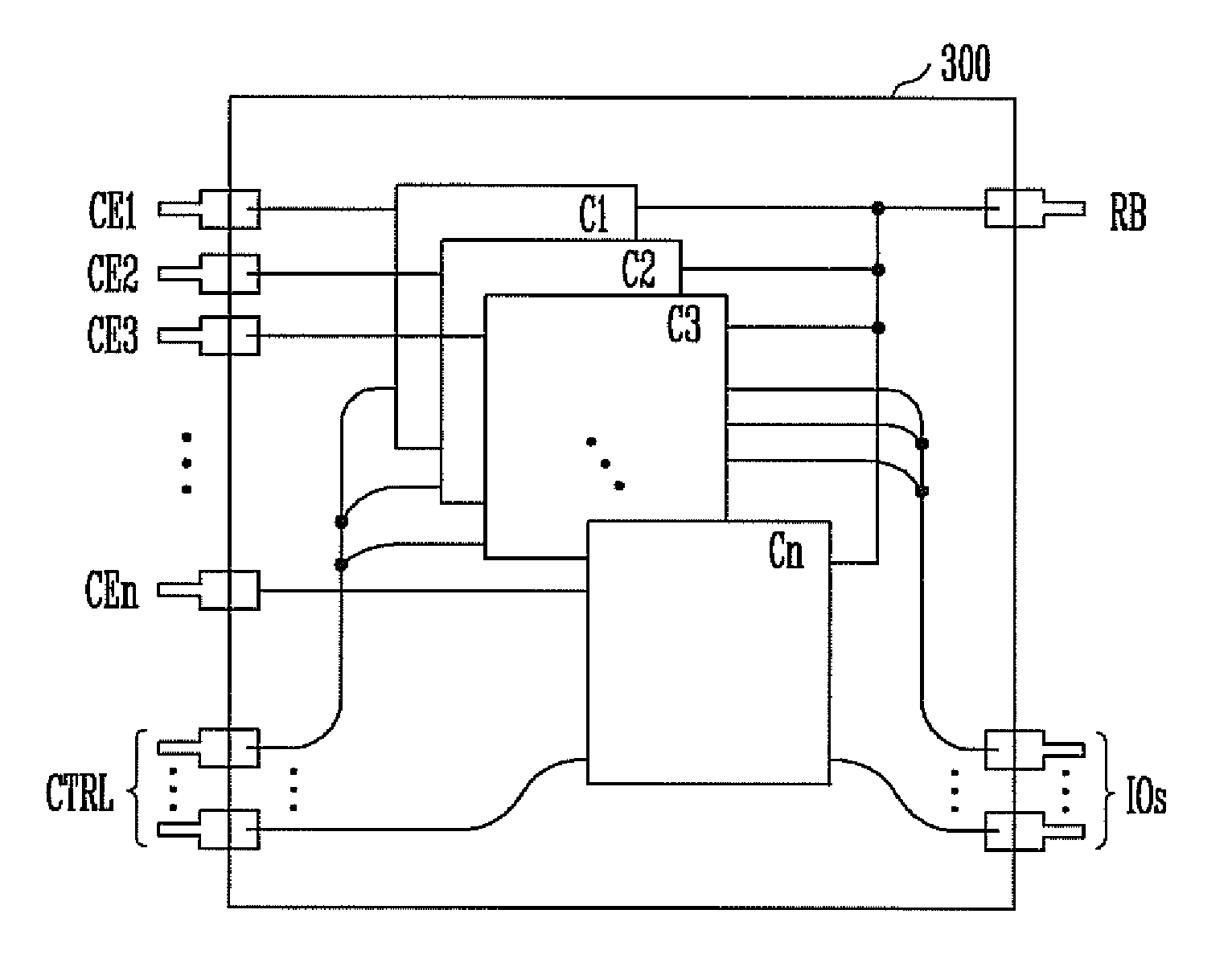
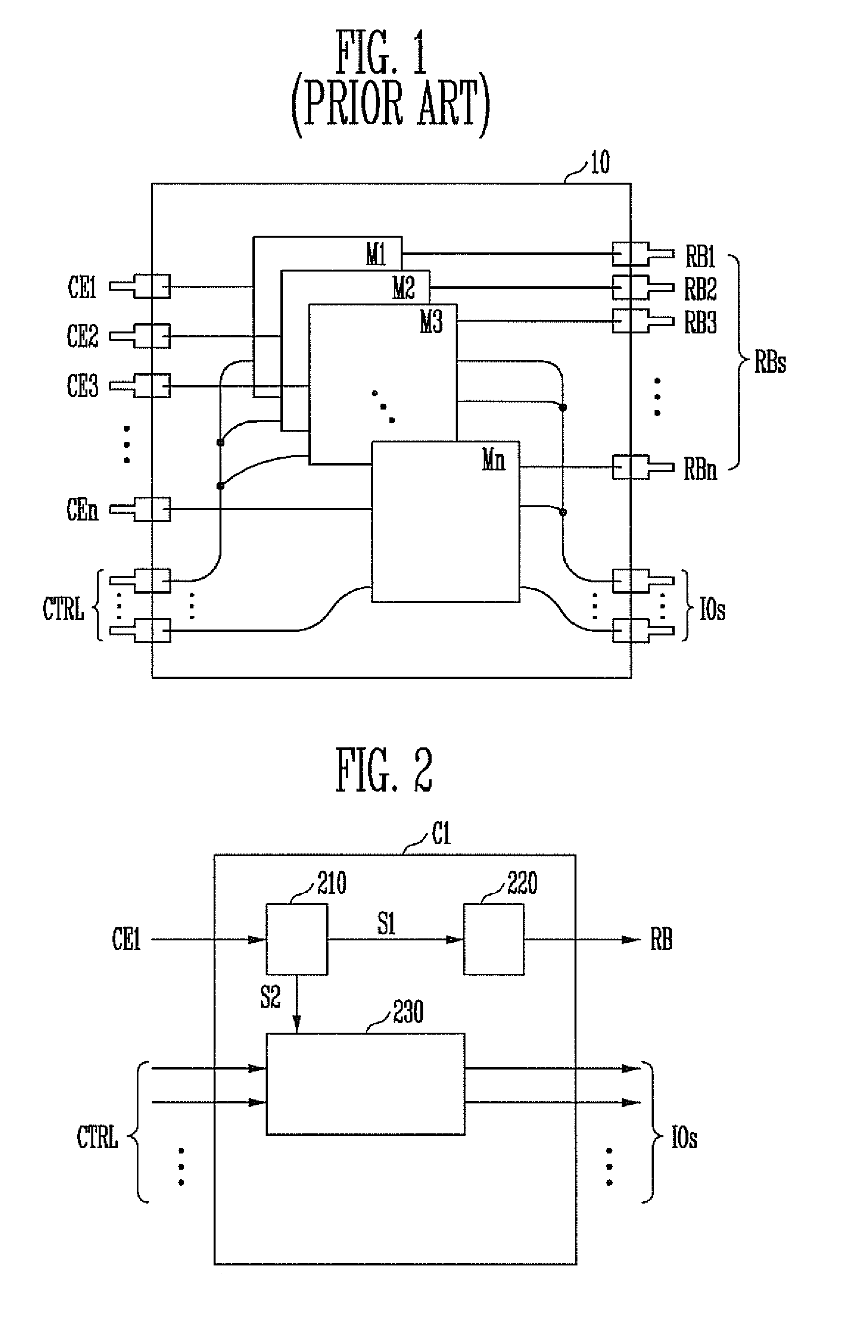
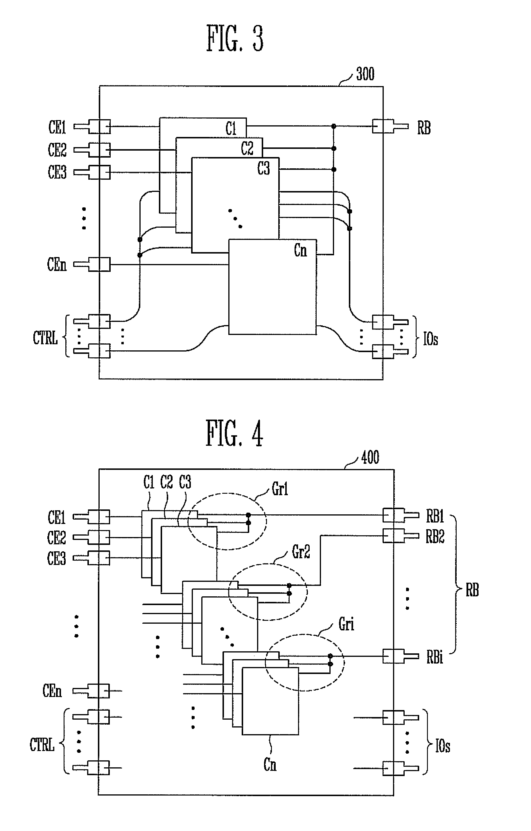
[0026]FIG. 2 is a diagram illustrating a memory chip according to an embodiment of the present invention.

[0027]Referring to FIG. 2, the memory chip C1 includes a chip enable detection unit 210, a chip operation detection unit 220, and an internal circuit 230. When a chip enable signal CE1 is supplied to the memory chip C1, the chip enable detection unit 210 outputs a first signal S1 to the chip operation detection unit 220 and a second signal S2 to the internal circuit 230. To this end, the chip enable detection unit 210 includes a terminal to which the chip enable signal CE1 is supplied. In response to the first signal S1, the chip operation detection unit 220 outputs an operation state signal RB indicating that ...


PUM


Abstract

A semiconductor memory device having a number of chips, each of the chips including a chip enable detection unit configured to simultaneously output a first signal and a second signal in response to a chip enable signal, a chip operation detection unit configured to output an operation state signal in response to the first signal, and an internal circuit configured to operate in response to a power source voltage and a control signal in response to the second signal being received.

Description

CROSS-REFERENCE TO RELATED APPLICATION[0001]Priority to Korean patent application number 10-2009-0047816 filed on May 29, 2009, the entire disclosure of which is incorporated by reference herein, is claimed.BACKGROUND[0002]One or more embodiments of the present invention relate to a semiconductor memory device and, more particularly, to semiconductor memory chips having a reduced number of pins outputting operation state signals.[0003]Recently, in line with the user's needs, semiconductor devices have been reduced in size and weight. Accordingly, with a reduction in the size of the semiconductor devices, semiconductor memory devices in which a number of memory chips are formed in a single semiconductor package are being developed.[0004]Each of the memory chips includes an internal circuit, including memory cells configured to store data and peripheral circuits configured to transfer driving voltages. The internal circuit is operated in response to a power source voltage, a chip enab...

Claims


Application Information

Patent Timeline
Patent Type & Authority Applications(United States)
IPC IPC(8): G11C5/06G11C7/00
CPCG11C5/063G11C5/06G11C7/10
Inventor WANG, JONG HYUN
Owner SK HYNIX INC
Why Eureka
Try Eureka