SRAM memory cell with double gate transistors provided with means to improve the write margin

a memory cell and double gate technology, applied in the field of sram memory cells, can solve the problems of increasing the difficulty of achieving a good compromise between these two factors, affecting the read stability of the memory cell formed of the transistor, and affecting the design of the memory cell in relation to the intended application

Inactive Publication Date: 2010-12-16
COMMISSARIAT A LENERGIE ATOMIQUE ET AUX ENERGIES ALTERNATIVES
View PDF5 Cites 18 Cited by
  • Summary
  • Abstract
  • Description
  • Claims
  • Application Information

AI Technical Summary

Benefits of technology

[0079]According to one possibility, the first access transistor may comprise a second gate electrode connected to the second storage node, the second access transistor comprising a second gate electrode connected to the first storage node. Said configuration may allow improved read stability.

Problems solved by technology

The two first criteria are difficult to reconcile with the last criterion, and lead memory designers to making compromises in relation to the intended applications.
This results in degradation of the electric characteristics of the memory cells formed of said transistors.
Two factors assume particular importance; the write margin (WM) and the static noise margin (SNM) insofar as, with respect to transistor technologies with gates of critical size of less than 45 nm also called >, it is increasingly more difficult to arrive at a good compromise between these two factors, notably on account of the increase in variations of methods used and the increase in leakage currents related to short channel effects.
Its disadvantages are: in particular an increase in occupied surface area and increased control complexity.
Nonetheless, it also has the effect of reducing second order stability by deteriorating the maintaining of node L.
The problem arises of finding a novel structure for double gate SRAM cell, in particular having 6 transistors, in which the compromise between read stability and write margin is improved.

Method used


Image

  • SRAM memory cell with double gate transistors provided with means to improve the write margin
  • SRAM memory cell with double gate transistors provided with means to improve the write margin
  • SRAM memory cell with double gate transistors provided with means to improve the write margin

Examples


Embodiment Construction

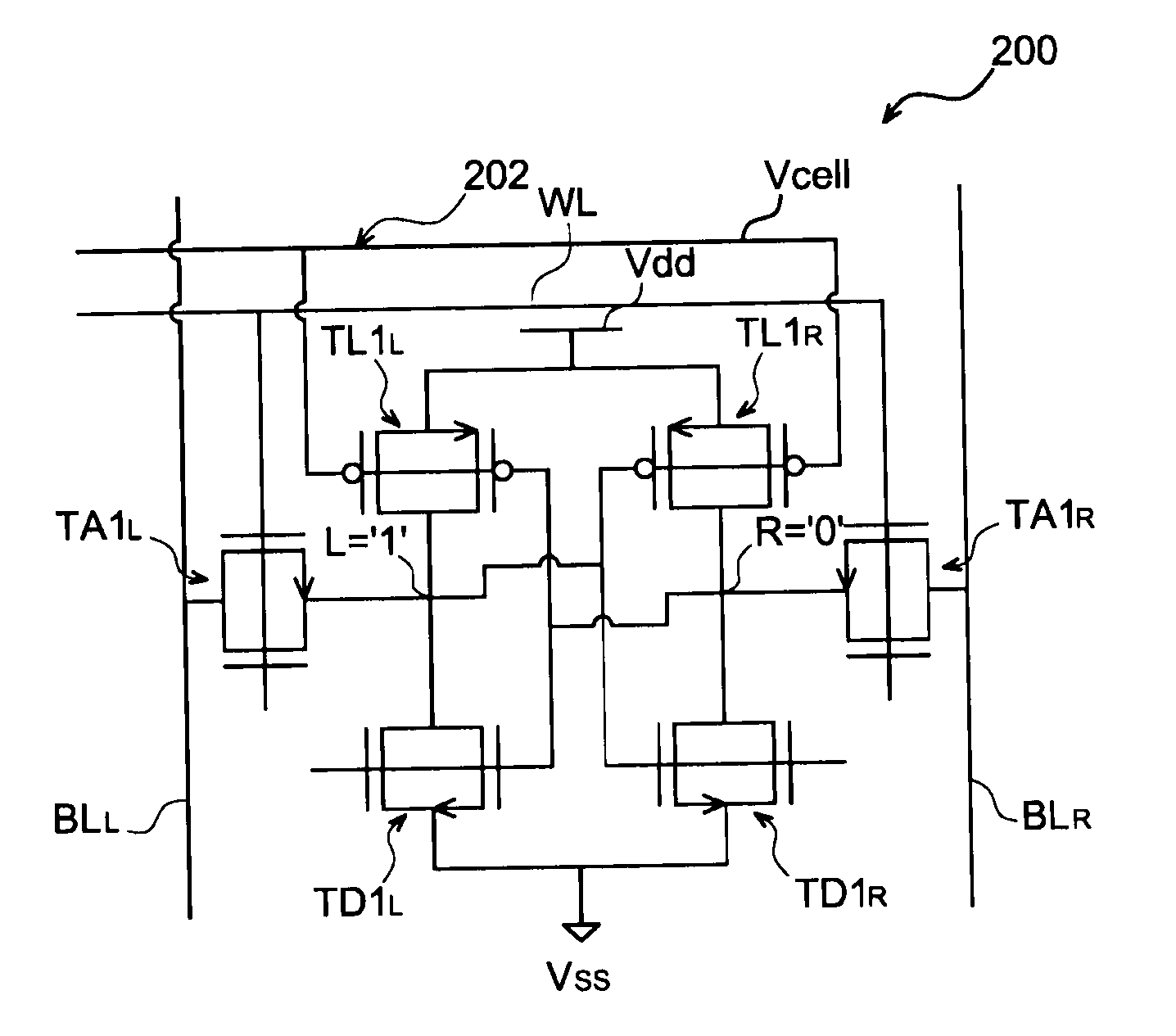
[0104]FIG. 8 gives an example of cell 200, with transistors (or > cell) of a memory of SRAM type. The cell 200 is formed of transistors fabricated using MOS technology (Metal Oxide Semi-conductor) and with double gate.

[0105]The cell 200 is provided with a first access transistor TA1L with double gate, and a second access transistor TA1R with double gate, which can be fabricated using a first given type of MOS technology, for example NMOS technology.

[0106]The first access transistor TA1L depending on the manner in which it is polarized, is designed to allow access or to block access to a first storage node L intended to hold given logic data, for example logic ‘1’. The second access transistor TA1R depending on the manner in which it is polarized, is designed to allow access or to block access to a second storage node R intended to hold logic data complementing said given logic data, for example logic ‘0’.

[0107]In this example, the two gates of the first access transistor TA1L and of...


PUM


Abstract

A random access memory cell including: two double-gate access transistors respectively arranged between a first bit line and a first storage node and between a second bit line and a second storage node, a word line, a first double-gate load transistor and a second double-gate load transistor, a first double-gate driver transistor and a second double-gate driver transistor, a mechanism to apply a given potential to at least one electrode of each of the load or driver transistors, and a mechanism to cause the given potential to vary.

Description

TECHNICAL AREA[0001]The invention relates to the area of Random Access Memories (RAMs) and particularly concerns a special structure of static memory cell with random access provided with double gate transistors.[0002]Said structure is notably provided with means to improve the write margin (WM) of the cell.[0003]The invention also concerns a memory comprising a plurality of said cells.STATE OF THE PRIOR ART[0004]A conventional SRAM memory cell (Static Random Access Memory) generally comprises two inverters, connected in a so-called <<flip-flop>> configuration and two access transistors connected to so-called bit lines and controlled by a word line.[0005]The desired characteristics for a memory cell are:[0006]good stability during different operations: read, write, retention, performed on the cell,[0007]a drive or load current that is as strong as possible to impart high operating speed to the cell,[0008]the lowest possible current in retention mode to minimize static co...

Claims


Application Information

Patent Timeline
Patent Type & Authority Applications(United States)
IPC IPC(8): G11C7/00
CPCG11C11/412
Inventor THOMAS, OLIVIERGIRAUD, BASTIEN
Owner COMMISSARIAT A LENERGIE ATOMIQUE ET AUX ENERGIES ALTERNATIVES
Why Eureka
Try Eureka