Independent-gate controlled asymmetrical memory cell and memory using the cell

a technology of independent gate control and asymmetric memory, applied in the field of electronic memory circuits, can solve the problems of significant threshold voltage fluctuation, deterioration of static random access memory (sram), and poor stability of conventional sram during read mode, and achieve the effect of improving read stability

Inactive Publication Date: 2007-08-30
GLOBALFOUNDRIES INC
View PDF7 Cites 5 Cited by
  • Summary
  • Abstract
  • Description
  • Claims
  • Application Information

AI Technical Summary

Benefits of technology

[0008] Principles of the present invention provide techniques for independent-gate controlled asymmetrical SRAM cells and SRAMS using the cells. Cells according to the present invention can obtain improved read stability.

Problems solved by technology

As device size substantially shrinks in advanced very large scale integration (VLSI) technology, increased process variation causes significant amounts of threshold voltage fluctuation.
As a result, stability of static random access memory (SRAM) deteriorates due to large threshold voltage mismatches between two neighboring transistors in a cell.
The conventional SRAM has its worst stability during the READ mode because the voltage at the storage node having a “zero” logic value rises during the READ cycle.
If this increased node voltage is larger than the trip voltage of the inverter, the stored logic values will be flipped and data will be lost.
While the so-called asymmetrical SRAM cell can achieve an improved static noise margin (SNM) as compared to a conventional symmetrical SRAM cell, there are practical limits, due to device size considerations, to obtaining further improvement in the SNM.

Method used


Image

  • Independent-gate controlled asymmetrical memory cell and memory using the cell
  • Independent-gate controlled asymmetrical memory cell and memory using the cell
  • Independent-gate controlled asymmetrical memory cell and memory using the cell

Examples


Embodiment Construction

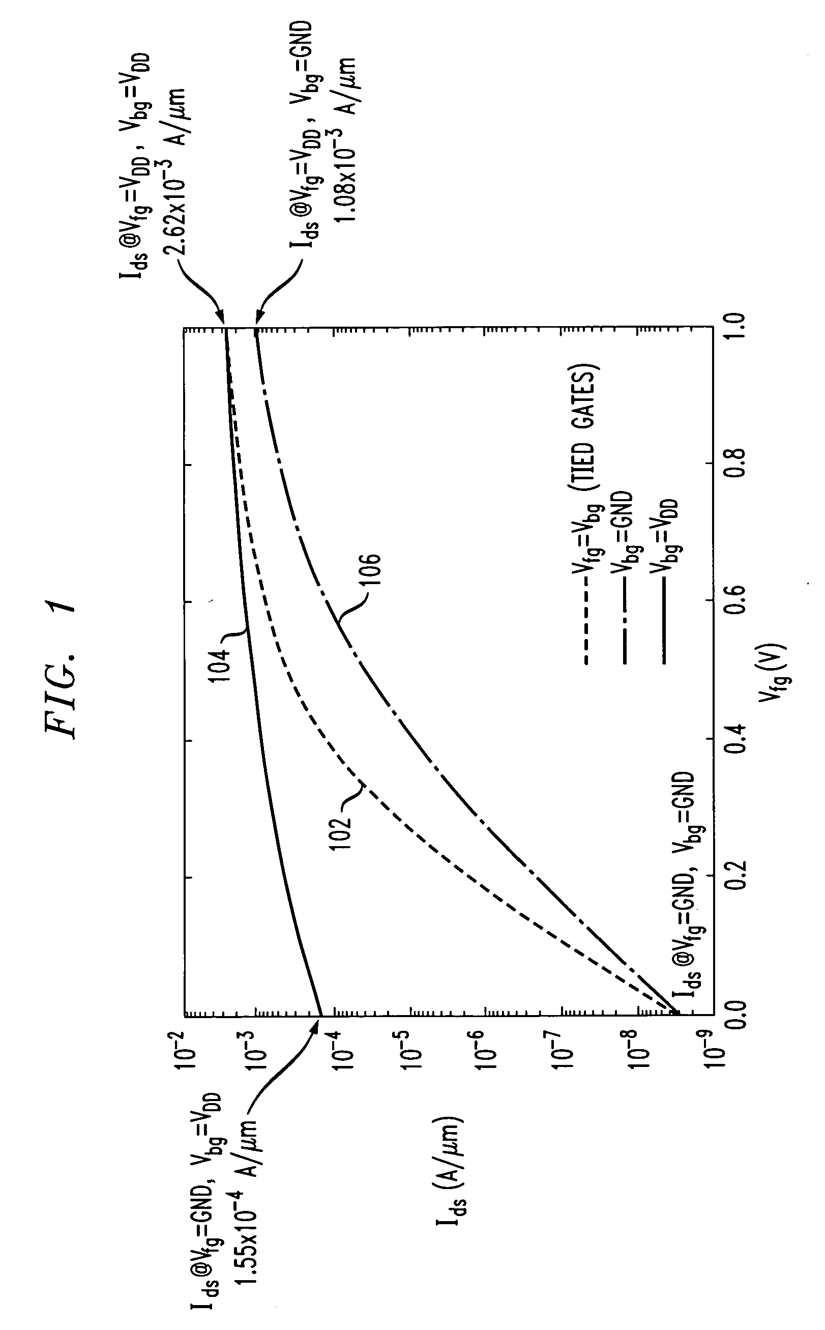
[0022] It is useful to refer to FIG. 1 and to consider the drain-to-source current (Ids) versus gate-to-source voltage (Vgs) characteristics of an asymmetrical double gate MOSFET with independent gate control. The Ids versus the front gate voltage (Vfg) characteristic is significantly different depending on the back gate voltage (Vbg). FIG. 1 depicts the Ids-Vfg curves 102, 104, 106 for, respectively the tied front and back gate, Vbg=VDD, and Vbg=ground cases. In each case, the devices have the same effective channel length (Leff=25 nm), identical front-gate and back-gate oxide thicknesses of 1 nm, and a film thickness of 7 nm. The body is undoped.

[0023] As shown in FIG. 1, we can have three different on-current values depending on the gate voltage setup. The case of the tied gates has the largest “on” current due to the coupling between the front and back gates. The case where the front gate is maintained at the supply voltage and the back gate is grounded has a larger current tha...


PUM


Abstract

Techniques are provided for employing independent gate control in asymmetrical memory cells. A memory circuit, such as an SRAM circuit, can include a number of bit line structures, a number of word line structures that intersect the bit line structures to form a number of cell locations, and a number of asymmetrical memory cells located at the cell locations. Each of the asymmetrical cells can be selectively coupled to a corresponding one of the bit line structures under control of a corresponding one of the word line structures. Each of the cells can include a number of field effect transistors (FETS), and at least one of the FETS can be configured with separately biased front and back gates. One gate can be biased separately from the other gate in a predetermined manner to enhance read stability of the asymmetrical cell.

Description

STATEMENT REGARDING FEDERALLY SPONSORED RESEARCH OR DEVELOPMENT [0001] This invention was made with Government support under contract number NBCH 3039004 awarded by the Defense Advanced Research Projects Agency (DARPA). The government has certain rights in this invention.FIELD OF THE INVENTION [0002] The present invention generally relates to electronic circuitry and, more particularly, to electronic memory circuits. BACKGROUND OF THE INVENTION [0003] As device size substantially shrinks in advanced very large scale integration (VLSI) technology, increased process variation causes significant amounts of threshold voltage fluctuation. As a result, stability of static random access memory (SRAM) deteriorates due to large threshold voltage mismatches between two neighboring transistors in a cell. The well-known conventional six transistor SRAM is described, e.g., in Hodges & Jackson's textbook “Analysis and Design of Integrated Circuits,” 2d edition, at pages 364-68 (New York, McGraw H...

Claims


Application Information

Patent Timeline
Patent Type & Authority Applications(United States)
IPC IPC(8): G11C11/00
CPCG11C11/412
Inventor CHUANG, CHING-TEKIM, JAE-JOONKIM, KEUNWOO
Owner GLOBALFOUNDRIES INC
Why Eureka
Try Eureka