Static Random Access Memory Cell

a random access memory and random access technology, applied in the field of static random access memory cells, can solve the problems of unselected data being turned, current leakage, and the integrated circuit design of the eight-transistor static random access memory cell incurs a higher complexity, so as to reduce the complexity of the integrated circuit design, increase the read bit line swing, and improve the accuracy of reading data. the effect of accuracy

Active Publication Date: 2013-05-02
NATIONAL TSING HUA UNIVERSITY
View PDF2 Cites 7 Cited by
  • Summary
  • Abstract
  • Description
  • Claims
  • Application Information

AI Technical Summary

Benefits of technology

[0019](1) With the third transistor, the SRAM cell forms a read port transistor, such that the memory cell has a read port capable of reading and writing memory cell independently, so as to eliminate the read disturb of the data voltage and the half-selected disturb of adjacent memory cells when the SRAM cell reads data, to enhance the accuracy and the hit rate of reading data.
[0020](2) The SRAM cell is an independent access memory cell formed by coupling seven transistors, and therefore, compared with the conventional eight-transistor SRAM cell, the seven-transistor SRAM cell can reduce the complexity of the integrated circuit design of the SRAM cell and the unit area of the memory cell.
[0021](3) With the third transistor, the SRAM cell forms a read port transistor, and with the fabrication method or post fabrication method, the read port transistor has a feature of an asymmetric threshold voltage, which can increase the read bit line swing, so as to enhance the sensing margin and read stability.
[0022](4) With the third transistor, the SRAM cell forms a read port transistor, and through boost the voltage of the read bit line, the sensing margin and read stability can be enhanced.

Problems solved by technology

As a result, the current is leaked, and data of adjacent unselected memory cells may be turned over in a serious case, and this phenomenon is called “half-selected disturb”.
However, the eight-transistor static random access memory cell achieves the effect of having independent read port and write port by means of the additional two pass gates, the pair of complementary read bit lines and a read word line, so that the integrated circuit design of the eight-transistor static random access memory cell incurs a higher complexity, an increased unit area and a higher power consumption.
In addition, the swing amplitude of the read bit line may be restricted by the data of the memory cells, so that the eight-transistor static random access memory cell may have a lower sensing margin, a lower read stability, a higher operation voltage and a higher power consumption.

Method used


Image

  • Static Random Access Memory Cell
  • Static Random Access Memory Cell
  • Static Random Access Memory Cell

Examples


Embodiment Construction

[0027]The technical characteristics and effects of the present invention will become apparent by the detailed description of preferred embodiments and related drawings as follows. For simplicity, same numerals are used to represent respective elements in the preferred embodiment and drawings.

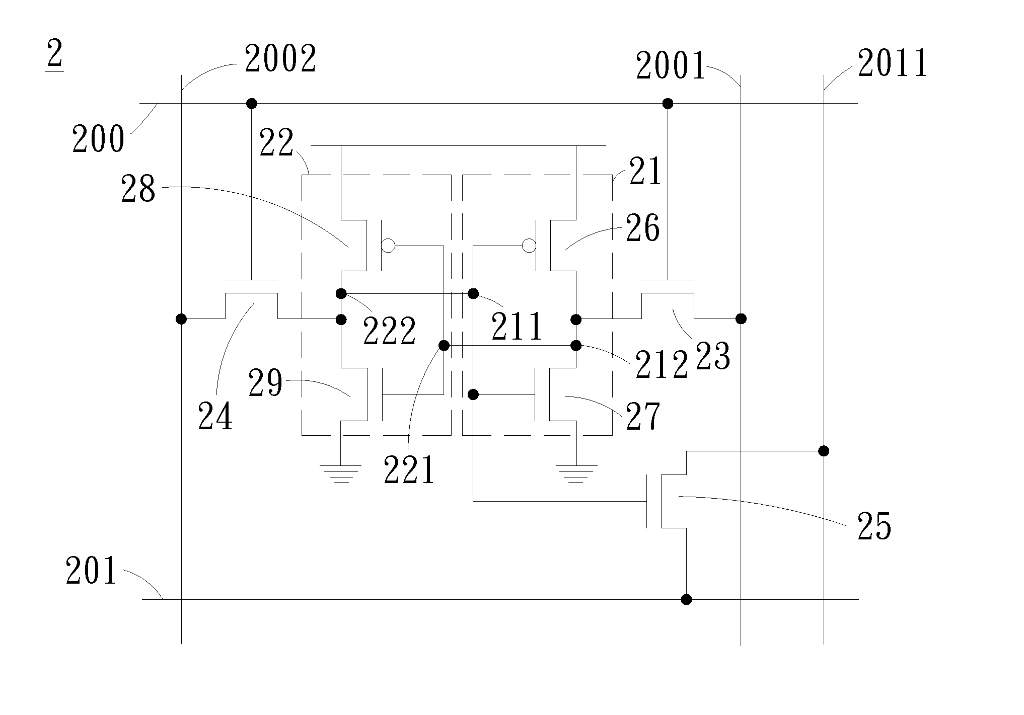
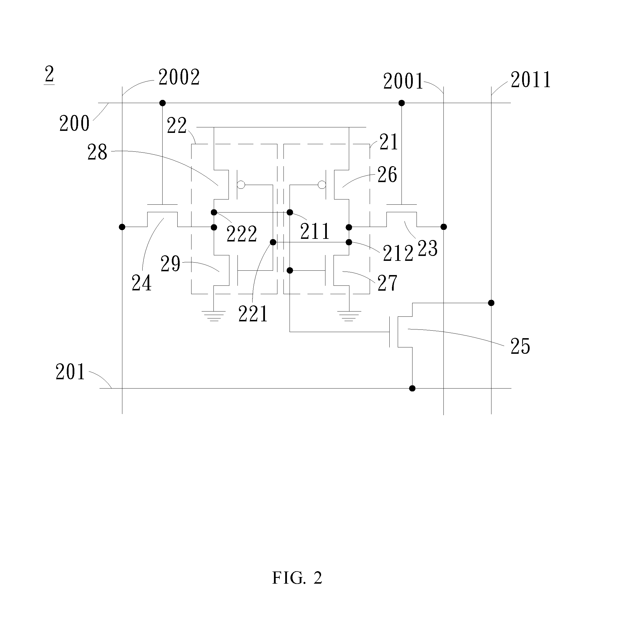
[0028]With reference to FIG. 2 for a schematic view of a SRAM cell in accordance with the first preferred embodiment of the present invention, the SRAM cell is a seven-transistor SRAM cell 2 comprising a first inverter 21, a second inverter 22, a first transistor 23, a second transistor 24 and a third transistor 25. The first inverter 21 includes a first input node 211 and a first output node 212, and the second inverter 22 includes a second input node 221 and a second output node 222. The first inverter 21 and the second inverter 22 are cross-coupled. In other words, the first output node 212 is coupled to the second input node 221, and the second output node 222 is coupled to the first input n...


PUM


Abstract

A static random access memory cell comprising a first inverter, a second inverter, a first transistor, a second transistor, and a third transistor. The first inverter is cross-coupled with the second inverter. The first transistor is connected with a write word line, a write bit line, and a first output node of the first inverter. The second transistor is connected with a complementary write bit line, the write word line, and a second output node of the second inverter. The third transistor is connected with a read bit line, a read word line, and the first input node of the first inverter to form a read port transistor, and a read port is formed. The read port transistor has a feature of asymmetric threshold voltage, and the read bit line swing can be expanded by the decrease of clamping current or the boosted read bit line.

Description

BACKGROUND OF THE INVENTION[0001]1. Field of the Invention[0002]The present invention relates to a semiconductor memory cell, in particular to a static random access memory cell (SRAM cell) formed by coupling seven transistors.[0003]2. Description of the Related Art[0004]Static random access memory (SRAM) has the advantages of quick access and low power consumption, and thus the SRAM is used extensively in electronic products including notebook computers, mobile devices and game players.[0005]Wherein, a conventional static access memory cell with a six-transistor (6T) structure is formed by six metal oxide semiconductor field effect transistors (MOSFET) coupled to one another. With reference to FIG. 1 for a schematic view of a conventional six-transistor SRAM cell, the six-transistor SRAM cell (6T-SRAM Cell) 1 comprises a first inverter 11, a second inverter 12, a first transistor 13 and a second transistor 14. The first inverter 11 and the second inverter 12 are formed by cross-cou...

Claims


Application Information

Patent Timeline
Patent Type & Authority Applications(United States)
IPC IPC(8): G11C11/40
CPCG11C11/412
Inventor CHANG, MENG-FANCHEN, LAI-FUWU, JUI-JENYAMAUCHI, HIROYUKI
Owner NATIONAL TSING HUA UNIVERSITY
Why Eureka
Try Eureka