Read stability of a semiconductor memory

a semiconductor memory and read stability technology, applied in the field of data storage, can solve the problems of high probability of reading disturb and loss of stored value, and achieve the effect of facilitating data value storage, reducing the probability of reading disturb and facilitating wri

Active Publication Date: 2012-07-05
ARM LTD
View PDF10 Cites 20 Cited by
  • Summary
  • Abstract
  • Description
  • Claims
  • Application Information

AI Technical Summary

Benefits of technology

[0033]In some embodiments the memory storage device may have an array of rows and columns of storage cells with data lines and complimentary data lines such as in a SRAM memory. In such a memory device both the data line and the complimentary data line of cells not being written to are pre-charged before the write request. Thus, one side of the storage cell will have a 0 stored on it and this will be different to the pre-charge value of one of the data lines. Once the data access device starts to conduct, the difference in voltage between the data line and the node of the storage cell storing a 0 will start to fall as the switching device starts to conduct. Determining the fall in the voltage level on the data line is one way of determining a suitable point at which to boost the predetermined voltage level and thereby facilitate a write while reducing the probability of a read disturb occurring on cells on the access control line that are not being written to.
[0034]A second aspect of the present invention provides a semiconductor memory storage device comprising: a plurality of storage cells for storing data each storage cell comprising an access control device for providing said storage cell with access to or isolation from a data line in response to an access control signal; access control circuitry for transmitting said access control signal along an access control line to control a plurality of said access control devices connected to said access control line; said access control circuitry being configured in response to a write request to write data to a selected storage cell connected to said access control line to transmit said access control signal by increasing a voltage level supplied to said access control line to a predetermined voltage level such that said access control devices connected said access control line provide their storage cells with access to said data line and after a delay to provide a boost to said predetermined voltage level to facilitate storage of a data value present on said data line in said selected storage cell; said access control circuitry comprising delay control circuitry for automatically determining said delay in dependence upon characteristics of said semiconductor memory device.
[0035]The present invention recognises that a side effect of word line boosting is the reduction of the access disturb margin, that is an increase in the probability of cells that are on the same access control line as the cell being written but are not themselves being written having their stored data value corrupted. It also recognises that, where there is a difference in data value between the value on the data line and the value held at a node in a storage cell connected to the data line the difference in voltage between these two points will be at its highest at a beginning of a write cycle. This difference will decrease as the write cycle progresses, and thus, it recognises that providing a delay to a boost signal boosting a voltage on a data access control line will reduce the maximum voltage difference seen by these two points and thereby reduce the probability of the non-selected cells having their stored values disturbed as the boost will occur when the difference in voltage levels between the stored value and the data line are not at their highest. It should be noted that the difference in voltage level between the data line and the cells not being written to will decay over the write cycle as the data line will not be held at the value it has thus, this value will change as charge sharing occurs.
[0036]A drawback of the delay is that it will increase the write cycle time. The boost to the access line voltage is provided to assist the write, and the sooner it is provided the sooner the write occurs and the less likely it is that the write will not have occurred within the write cycle time. The present invention recognises that by providing delay control circuitry for automatically determining the delay in dependence upon characteristics of the semiconductor memory device, it can provide a suitable delay to increase the read stability of the memory device to a required level while still providing an acceptable write time.

Problems solved by technology

The larger the charge injected, the higher the probability of the storage cell being disturbed and losing its stored value.

Method used


Image

  • Read stability of a semiconductor memory
  • Read stability of a semiconductor memory
  • Read stability of a semiconductor memory

Examples


Embodiment Construction

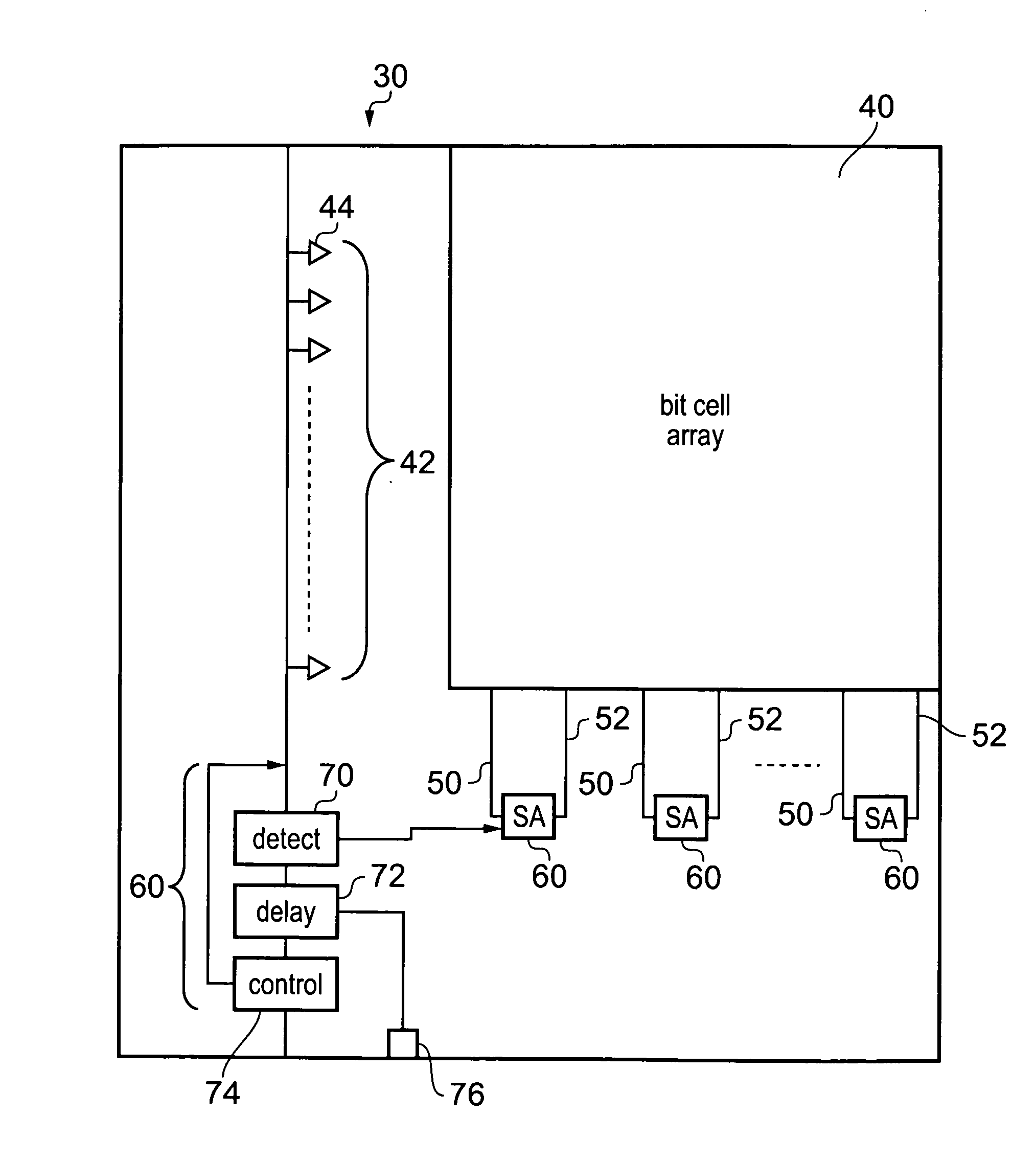
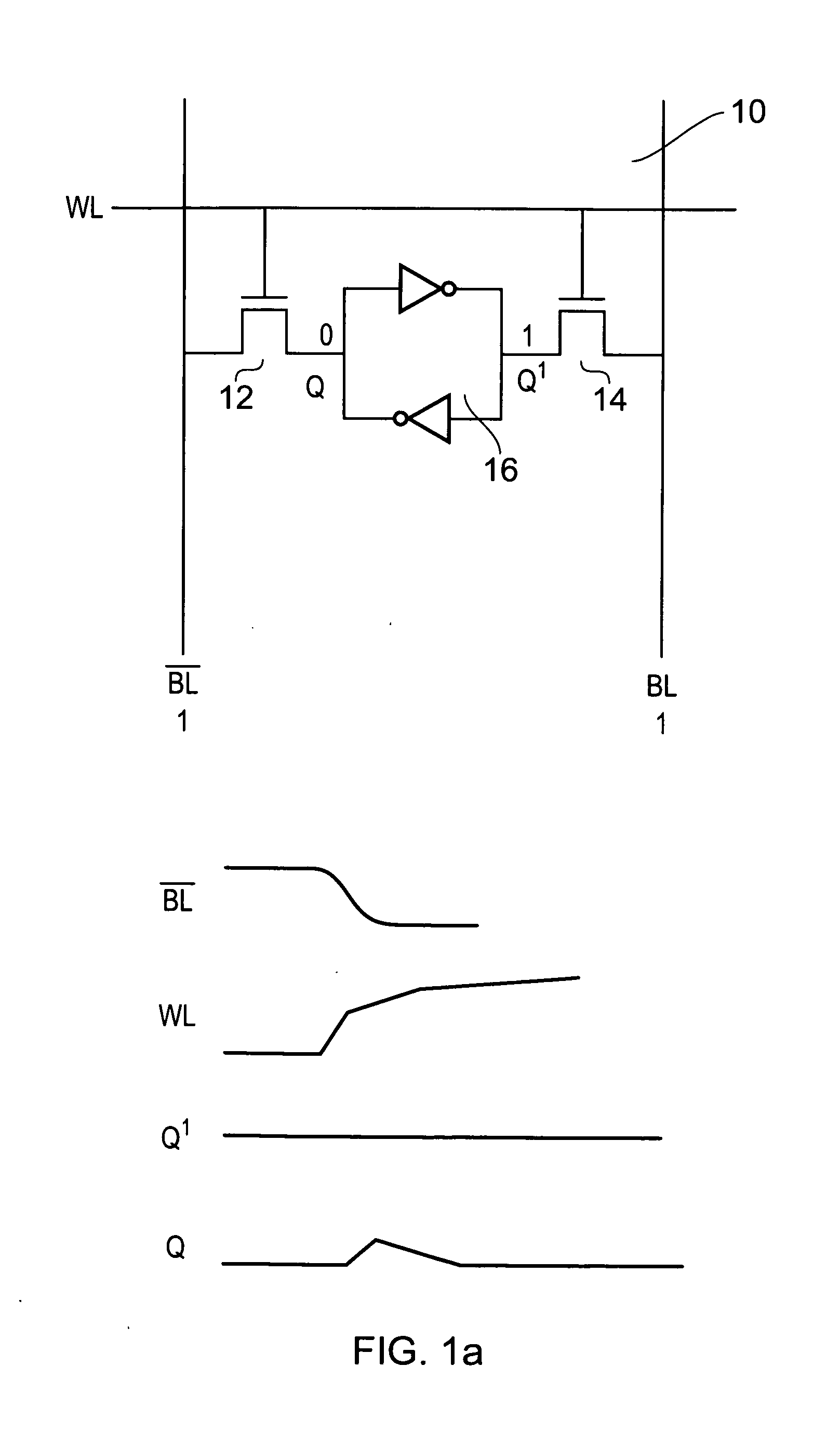
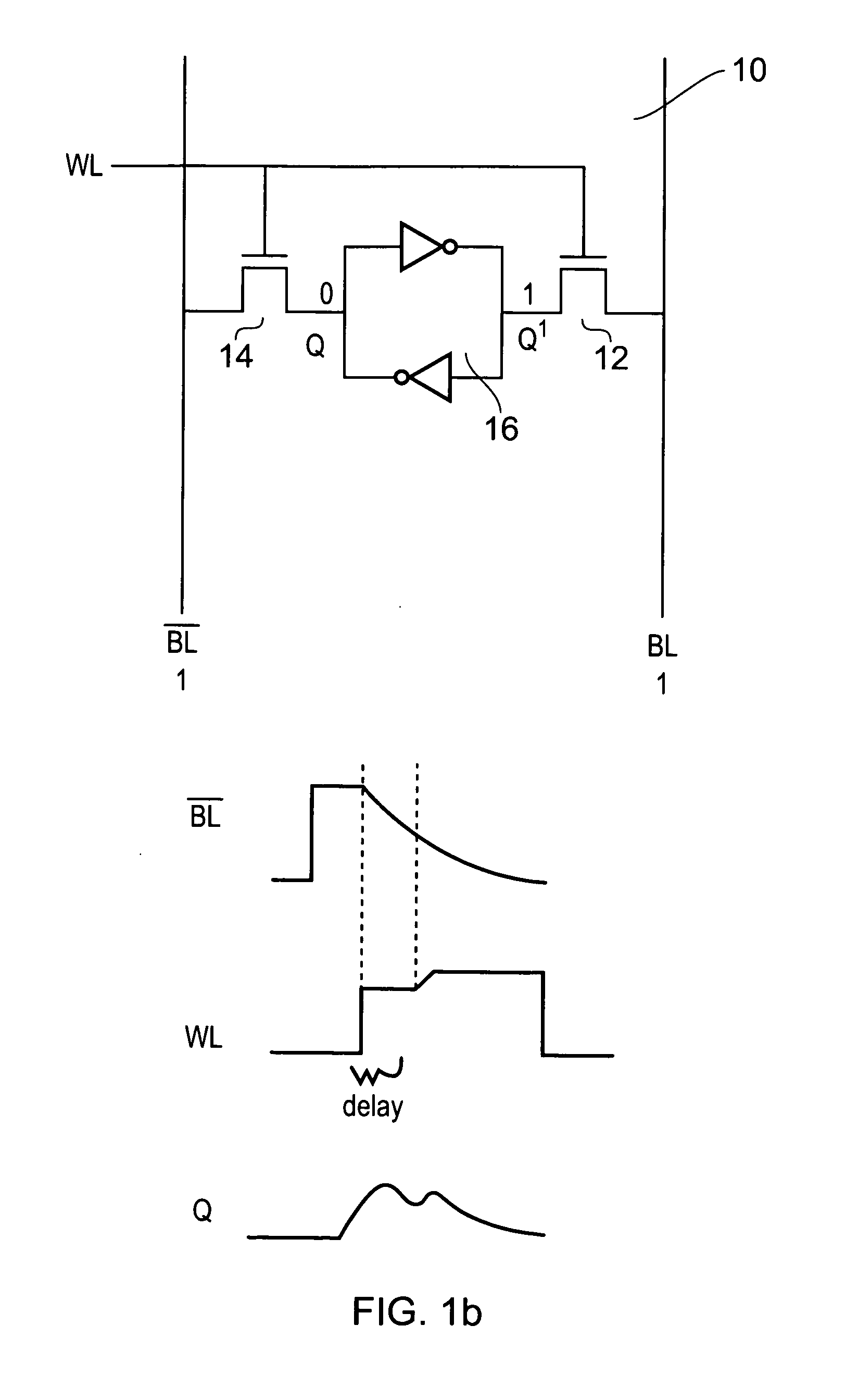
[0053]FIG. 1a shows a data storage cell 10 which is a conventional six transistor bit cell of a SRAM memory. This storage cell 10 has access control transistors 12 and 14 which provide access between the cross-coupled inverter storage cell 16 and the bit line BL and the complementary bit line BL.

[0054]These access control devices 12, 14 are controlled by a voltage level on the word line WL. Thus, if access to a row of storage cells 10 within a memory array is requested the voltage level on this word line is increased to a predetermined value corresponding to the high voltage rail of the circuit and the access control devices 12 and 14 which in this embodiment are transistors are turned on. Thus, the two nodes in the storage cell Q and Q′ are then connected to the complementary bit line and the bit line respectively.

[0055]Prior to the word line voltage level rising the bit line and complementary bit line of cells that are not being written to are pre-charged to hold a 1 level.

[0056]I...


PUM


Abstract

A semiconductor memory storage device is disclosed. The memory comprises a plurality of storage cells for storing data each storage cell comprising an access control device for providing the storage cell with access to or isolation from a data access port in response to an access control signal, access control circuitry for transmitting the access control signal along an access control line to control a plurality of the access control devices connected to the access control line. The access control circuitry responds to a data access request signal by increasing a voltage level supplied to the access control line to a first voltage level at a first average rate and then in response to receipt of a further signal increasing the voltage level supplied to the access control line to the predetermined higher voltage level, in such a way that a further average rate of increase of the voltage level from the first to the predetermined higher voltage level is lower than the first average rate of increase to the first level.

Description

BACKGROUND OF THE INVENTION[0001]1. Field of the Invention[0002]The field of the invention relates to the field of data storage and in particular, to the storage and access of data in semiconductor memories.[0003]2. Description of the Prior Art[0004]With ever increasing demands to reduce both the size of devices and their power consumption, it is becoming increasingly challenging to design robust semiconductor memories such as SRAM. Each storage cell in an SRAM comprises a feedback loop for holding a data value. In order to write to the feedback loop and store a new value, the input data value must have a high enough voltage level to be able to switch the state stored by the feedback loop if required, while reading from the feedback loop should be performed without disturbing the values stored in any of the feedback loops. When reading from a cell both bit lines are pre-charged and the side of the cell storing a 0 will pull down the bit line it is connected to and this change in vol...

Claims


Application Information

Patent Timeline
Patent Type & Authority Applications(United States)
IPC IPC(8): G11C7/22G06F17/50G11C7/12
CPCG11C7/222G11C11/413G11C11/418G11C11/41G11C11/412G11C8/16G11C11/419G11C8/10G11C8/08
Inventor IDGUNJI, SACHIN SATISHGAJJEWAR, HEMANGI UMAKANTSCHUPPE, VINCENT PHILLIPECHONG, YEW KEONGCHEN, HSIN-YU
Owner ARM LTD
Why Eureka
Try Eureka