[0009]In addition, each
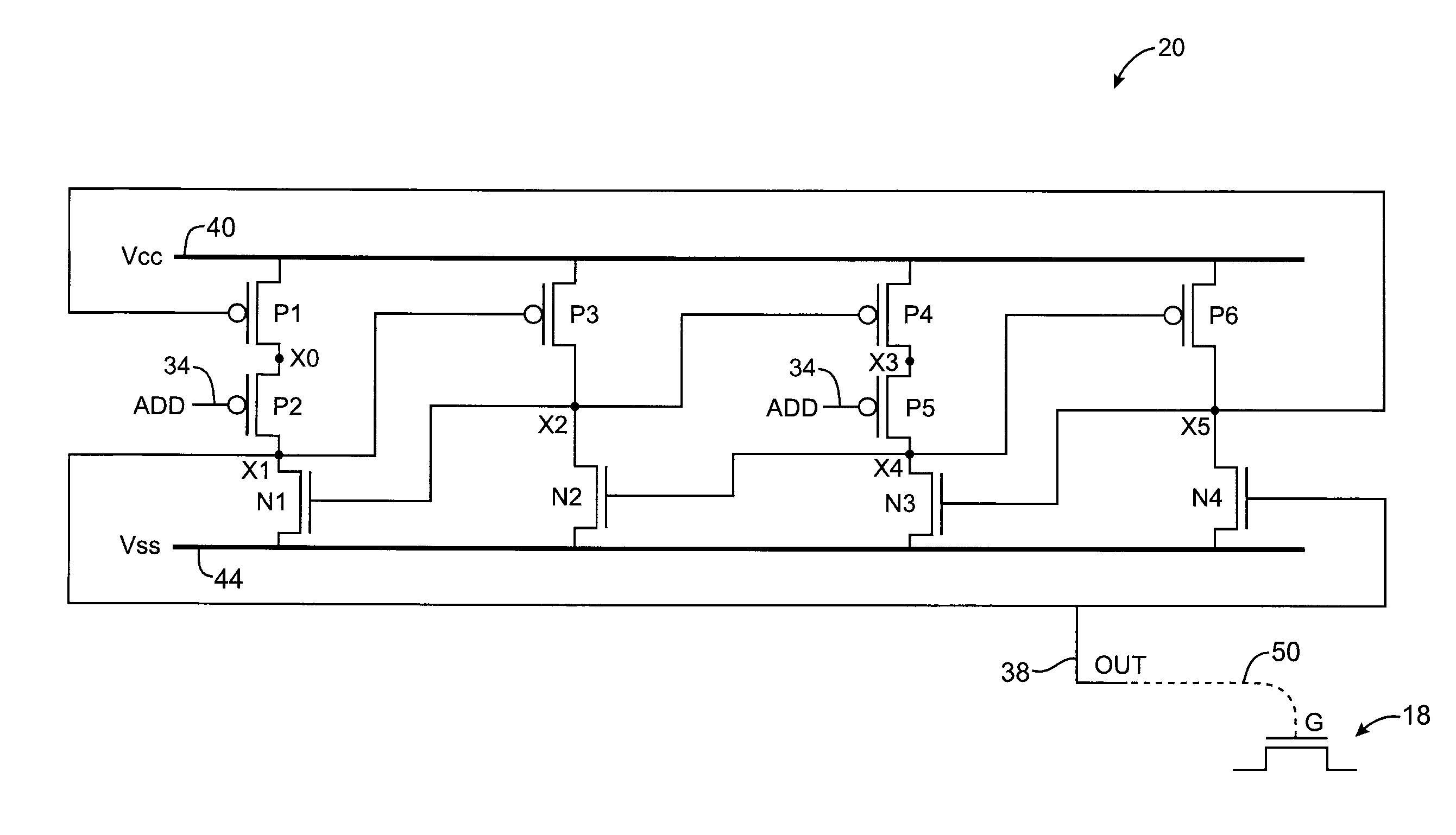
memory cell may have one or more control transistors (also sometimes referred to as write enable transistors, read-write control transistors, or write transistors) each of which is associated with a respective one of the transistor pairs. The control transistors can be coupled in series with the transistors in some or all of the transistor pairs. With one suitable arrangement, each of the control transistors may be a PMOS transistor coupled between the two transistors in a respective transistor pair. With another suitable arrangement, each of the control transistors may be a PMOS transistor coupled between a PMOS transistor in a respective transistor pair and a
positive power supply line (Vcc). If desired, some or all of the control transistors may be implemented using NMOS transistors. The control transistors may be controlled using one or more control signals such as address signals provided on address lines (word lines). When the control transistors are turned off (e.g., during write operations), the
memory cell is less resistant to state changes, which facilitates write operations.
[0011]Each
memory cell may have one or more address transistors. For example, each
cell may have a pair of address transistors. The address transistors may be controlled using a pair of address signals on respective address lines (word lines).
Data lines may be used to convey data to and from the memory cells. For example, a single data line (bitline) may be connected to the
cell through the pair of address transistors. During data writing operations, the address transistors may be controlled in parallel to load data into the memory
cell and the control signals for the two control transistors may be deasserted to temporarily decouple the PMOS and NMOS transistors in two of the transistor pairs in the memory cell (e.g., to disable the inverter-like circuits formed by the transistors in the transistor pairs associated with the control transistors). This weakens the cell's resistance to state changes and makes it easier to write data into the cell.
[0012]To enhance
write margin, the
power supply voltage to the cell may be lowered temporarily during writing and / or the address signals may be overdriven. If desired, data signals carried on the data line may be overdriven. For example, if data “1's” are normally represented by a Vcc value of 1.0 volts, the data write signals may have an
overdrive voltage of 1.2 volts (as an example). In general, overdriven signals may also include signals that are sometimes referred to as underdriven signals (e.g., signals with a normal ground
signal value of 0.0 volts that are “underdriven” to a
negative voltage such as −0.2 volts). Underdriving a
signal by lowering its ground
voltage in this way may enhance
write margin and therefore serves as a type of overdrive scheme.
[0014]If desired, memory cells may be provided that have fewer than four interconnected transistor pairs. For example, cells may be provided that have two interconnected transistor pairs (cross-coupled inverters) or three interconnected transistor pairs. As with cells based on four interconnected transistor pairs, cells with fewer interconnected transistor pairs may be provided with control transistors. During data read operations and during normal operation in a circuit, the control transistors may be turned on. In this configuration, the interconnected pairs of transistors form a bistable memory element that stores data. In a
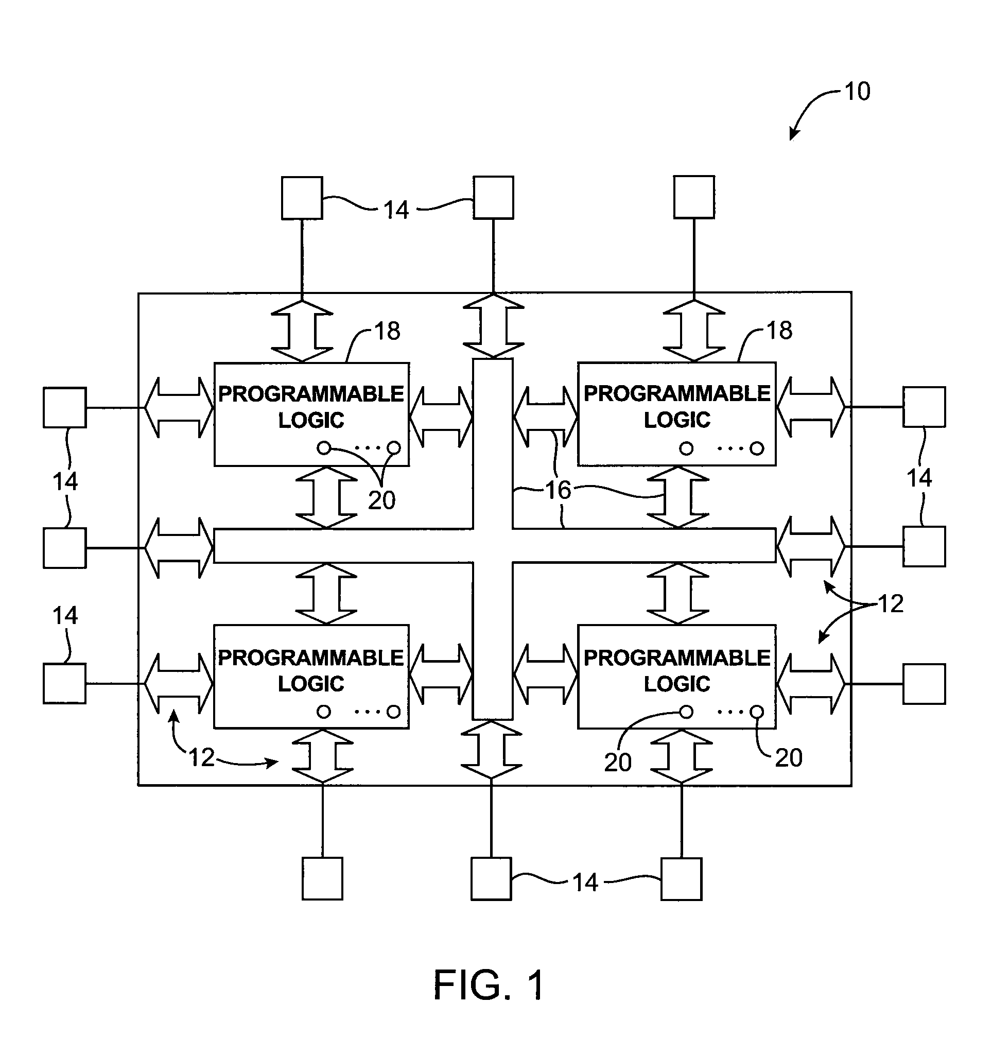
programmable logic device or other programmable circuit, for example, the bistable memory element may store configuration data for configuring programmable logic. The configuration data may be applied to the gate of a transistor or other programmable logic circuit element. During data write operations, the control transistors can be turned off. When the control transistors are off, the memory cell is made less stable and is less resistant to state changes. For example, it may be easier to write a logic “0” (e.g., data “zeros”) onto certain nodes in the cell because the transistors that would normally hold these nodes high are electrically disconnected when the control transistors are off. It may be easier to write a logic “1” (e.g., data “ones”) onto these nodes, because the logic “1” can be overdriven (e.g., represented by elevated positive voltages) without generating undesirable leakage currents into the
positive power supply rail.
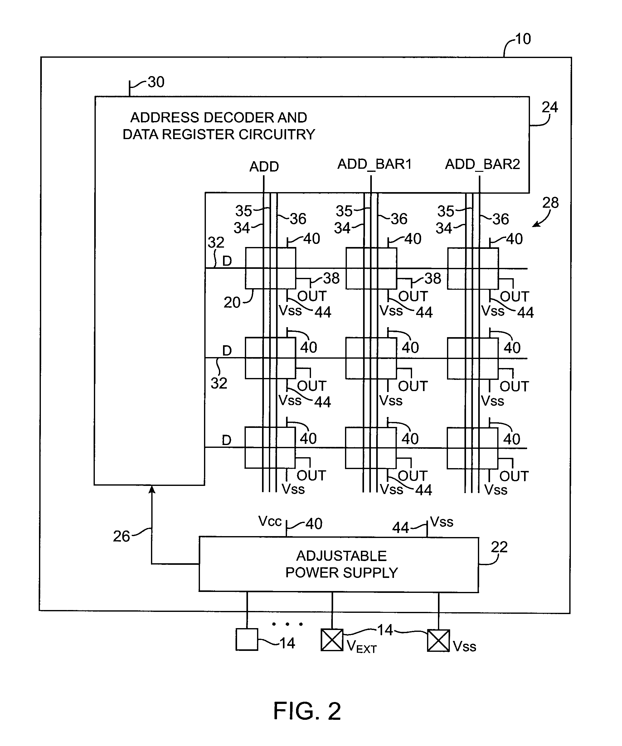
[0015]
Transistor layouts for the memory cells may be provided that create a
physical separation between the internal nodes in the cell. In the event of a
radiation strike in the vicinity of one node, the voltages on other nodes will not be immediately affected and will be able to help the cell recover without flipping its state. Spaces that are generated in the
layout pattern to create the
physical separation may be used for implementing other circuitry for the integrated circuit in which the memory cells are contained. For example, if the memory cell is being implemented as part of a programmable integrated circuit that uses configurable multiplexers, the transistor
layout for the memory cells can include
multiplexer transistors in the otherwise unoccupied spaces between the memory cell transistors. With one suitable arrangement, a transistor
layout may include two interleaved CRAM cells. This type of arrangement may allow internal nodes of the two CRAM cells to be physically separated in an efficient manner (e.g., without consuming excessive circuit area).

