SRAM cell

a memory and sram technology, applied in the field of memory, can solve the problems of non-negligent additional cost in terms of surface area and electric power consumption, and achieve the effects of increasing static noise margin or read stability, no additional cost, and increasing retention noise margin

Inactive Publication Date: 2018-09-27
COMMISSARIAT A LENERGIE ATOMIQUE ET AUX ENERGIES ALTERNATIVES
View PDF6 Cites 3 Cited by
  • Summary
  • Abstract
  • Description
  • Claims
  • Application Information

AI Technical Summary

Benefits of technology

[0014]Another object of an embodiment is for the provided SRAM to comprise assistance circuits with substantially no additional cost in terms of surface area.
[0015]Another object of an embodiment is for the SRAM cell to have an increased retention noise margin.
[0016]Another object of an embodiment is for the SRAM cell to have an increased static noise margin or read stability.
[0017]Another object of an embodiment is for the SRAM cell to have an increased write stability.
[0018]Another object of an embodiment is for the SRAM cell to have a low bulk.
[0019]Another object of an embodiment is for the minimum power supply voltage of the SRAM cell to be decreased.

Problems solved by technology

Since these criteria cannot all be satisfied, memory designers are led to making compromises therebetween.
However, this results in the addition of additional circuits in the memory, which may cause a non-negligible additional cost in terms of surface area and of electric power consumption.
The problem of finding a new SRAM cell structure having on the one hand a good retention noise margin, in read and write mode, while keeping a small bulk and a sufficient speed, is posed.

Method used


Image

  • SRAM cell
  • SRAM cell
  • SRAM cell

Examples


Embodiment Construction

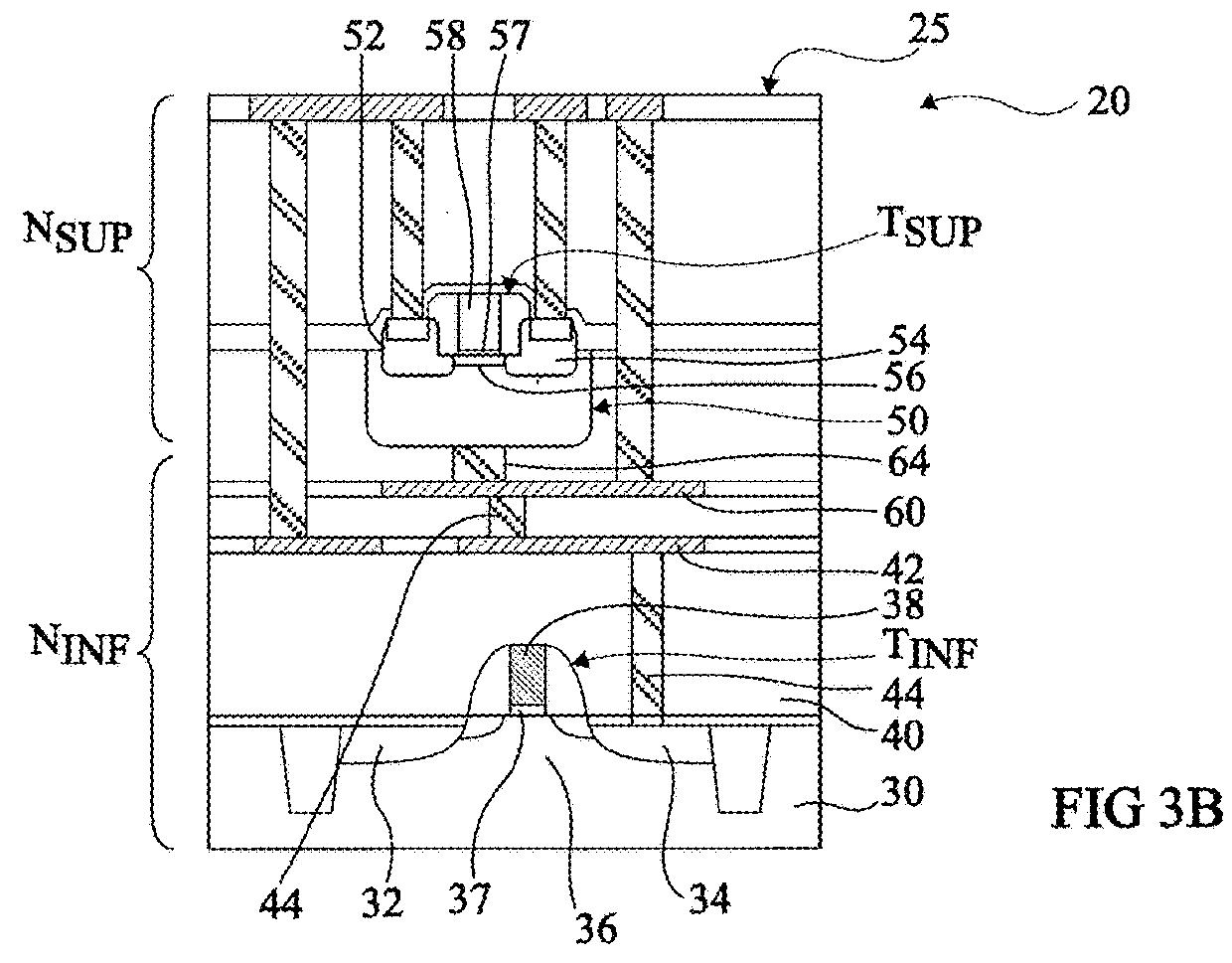
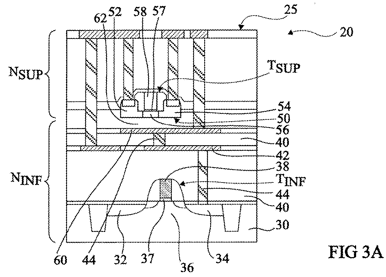
[0049]The same elements have been designated with the same reference numerals in the different drawings. For clarity, only those steps and elements which are useful to the understanding of the described embodiments have been shown and are detailed. The terms “approximately”, “substantially”, and “in the order of” are used herein to designate a tolerance of plus or minus 10%, preferably of plus or minus 5%, of the value in question.

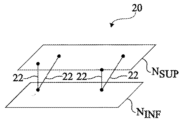
[0050]FIG. 2 very schematically shows an embodiment of an improved SRAM cell 20 comprising transistors, particularly metal oxide semiconductor field-effect transistors, currently called MOSFETs, formed in a stack of an electronic circuit over two levels of the stack. In particular, the memory cell comprises transistors located in an upper level NSUP, which have a threshold voltage capable of being modulated, the channel of each of the transistors being electrically coupled to a node of the electronic circuit of a lower level NINF via electrically-conductiv...


PUM


Abstract

A SRAM cell, including, in a stack of layers, transistors including at least first and second access transistors connected to a word line, the first access transistor coupling a first bit line and a first storage node and the second access transistor coupling a second bit line and a second storage node, and a flip-flop including a first conduction transistor coupling the first storage node to a source of a first reference potential and having its gate coupled to the second storage node and a second conduction transistor coupling the second storage node to the source of the first reference potential and having its gate coupled to the first storage node.

Description

BACKGROUND[0001]The present disclosure concerns memories, and particularly static random access memories, also called SRAM.DISCUSSION OF THE RELATED ART[0002]FIG. 1 shows a conventional SRAM cell comprising two inverters 10, 11 connected according to a so-called flip-flop configuration, and two access transistors 12, 13 connected to bit lines 15 and 16 and controlled by a word line 17.[0003]The characteristics desired for a memory cell are:[0004]a good static noise margin, SNM;[0005]a sufficient write margin, WM;[0006]a good retention noise margin, RNM;[0007]a conduction current, through access transistors 12, 13, which is as high as possible to give the cell a high operating speed;[0008]as small a cell size as possible to enable to form a memory with a significant cell integration density;[0009]as low a retention current as possible to minimize the consumed static power.[0010]Since these criteria cannot all be satisfied, memory designers are led to making compromises therebetween. ...

Claims


Application Information

Patent Timeline
Patent Type & Authority Applications(United States)
IPC IPC(8): G11C11/412H01L27/11
CPCG11C11/412H01L27/1104G11C5/02G11C11/417H01L27/0688H10B10/125H10B10/12
Inventor NOEL, JEAN-PHILIPPEAKYEL, KAYA CANGIRAUD, BASTIEN
Owner COMMISSARIAT A LENERGIE ATOMIQUE ET AUX ENERGIES ALTERNATIVES
Why Eureka
Try Eureka