Optical phase modulation element and optical modulator using the same

Inactive Publication Date: 2010-12-16
NEC CORP
View PDF1 Cites 15 Cited by
  • Summary
  • Abstract
  • Description
  • Claims
  • Application Information

AI Technical Summary

Benefits of technology

[0006]One object of the invention is to provide an optical phase modulation element and an optical modulator using the same, which can overcome at least one of the foregoing problems. One example of this object associated with an optical phase modulation element and an optical modulator using the same

Problems solved by technology

However, there are problems of expensive manufacturing costs as well as high integration, which are difficult to overcome.
This as a result causes a problem to the difficulty of high speed operation.
However, there is a very difficult problem of injecting incident light into the metal gap, which is much smaller than the wavelength of the incident light.
Thus, when a Mach-Zehnder interferometer is combined, an increasing length of the waveguide is required in order to increase the modulation ratio by setting the phase difference of two light beams to about π. This as a result causes problems such as an increasi

Method used


Image

  • Optical phase modulation element and optical modulator using the same
  • Optical phase modulation element and optical modulator using the same
  • Optical phase modulation element and optical modulator using the same

Examples


Example

First Embodiment

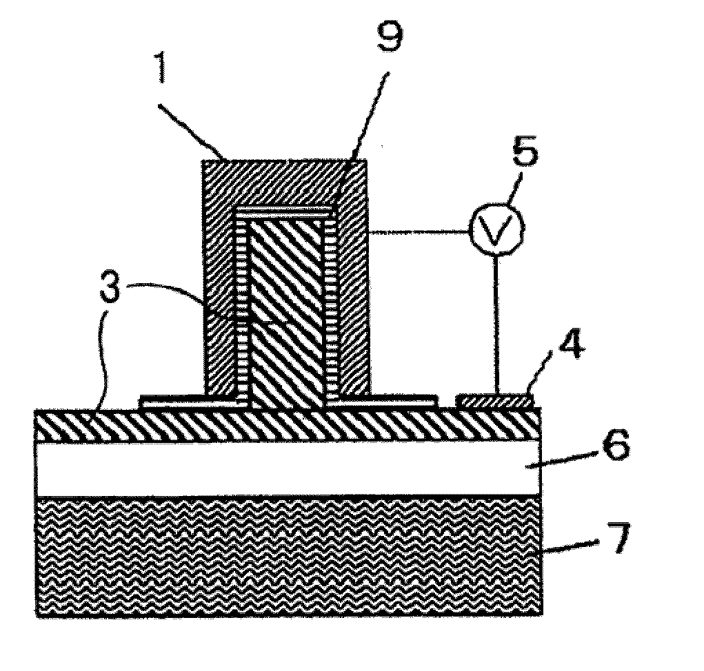
[0017]FIG. 1 is a cross-sectional view illustrating a Metal Insulator Semiconductor (MIS) type optical phase modulation element according to a first embodiment of the invention, taken in a direction crossing a waveguide direction. In this figure, embedded oxide layer 6 is formed on the principle surface of substrate 7, n-semiconductor 3 is formed on embedded oxide layer 6, and a part of n-semiconductor 3 opposite to substrate 7 is formed as a protrusion extending in one direction. Metal clad 1 is provided on the surface of n-semiconductor 3 including the protrusion, with insulating film 2 sandwiched between metal clad 1 and n-semiconductor 3. This structure is referred to as an MIS capacitor structure. In addition, due to this structure, a Plasmon waveguide is formed, in which the protrusion of n-semiconductor 3 and insulating film 2 act as a waveguide core and metal clad 1 acts as a waveguide clad, so that surface Plasmon polariton is guided in a direction perpendic...

Example

Second Embodiment

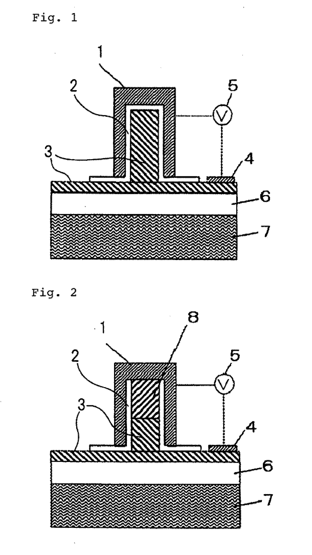
[0020]FIG. 2 is a cross-sectional view illustrating a P-N type optical phase modulation element according to a second embodiment of the invention, taken in a direction crossing a waveguide direction. As shown in the figure, this embodiment is different in a semiconductor structure forming a part of waveguide core from the MIS optical phase modulation element of the first embodiment. Specifically, p-semiconductor 8 is stacked on a protrusion of n-semiconductor 3, and metal clad 1 is provided on the protrusion with insulating film 2 sandwiched between metal clad 1 and the protrusion. In addition, the top surface of p-semiconductor 8 is not coated with insulating film 2 but is in close contact with metal clad 1. The other construction is the same as in the first embodiment.

[0021]The modulation element of this construction can modulate the equivalent refractive index of a Plasmon waveguide by changing carrier density when carriers are injected into P-N junction semicond...

Example

Third Embodiment

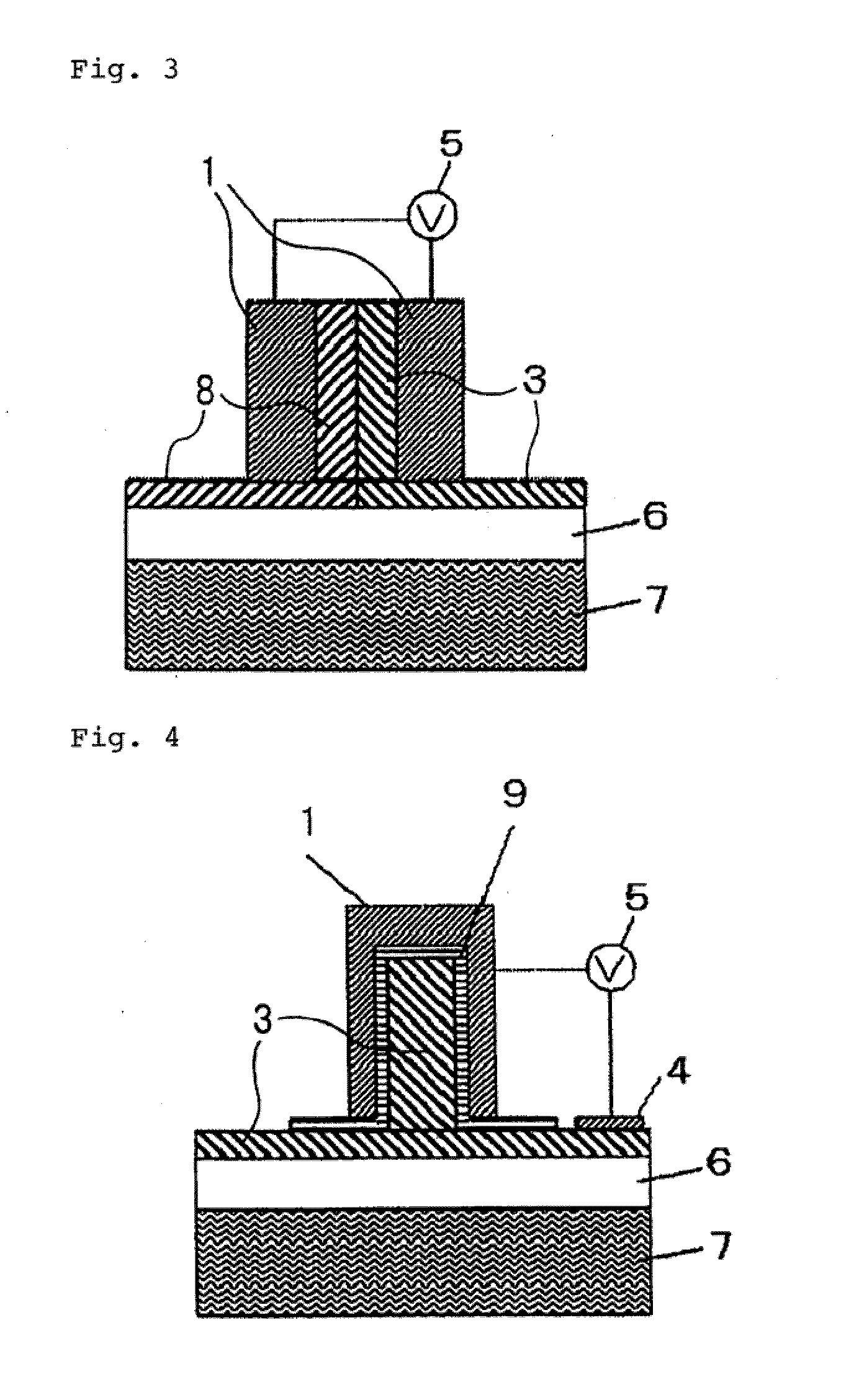
[0023]FIG. 3 is a cross-sectional view illustrating a P-N type optical phase modulation element according to a third embodiment of the invention, taken in a direction crossing a waveguide direction. As illustrated in the figure, this embodiment is different in a semiconductor structure of a waveguide core and a waveguide clad structure from the previous two embodiments. Specifically, n-semiconductor 3 and p-semiconductor 8 formed on embedded oxide layer 6 along the in-plane direction (i.e., the lateral direction in the figure) make a P-N junction structure. The semiconductor part having this P-N junction forms a protrusion that protrudes in a direction opposite to substrate 7. In addition, two metal clads 1 are disposed with both the right and left sides of the protrusion sandwiched between metal clads 1. Two metal clads 1 have a function as positive-negative electrodes, with one of metal clads 1 in close contact with n-semiconductor 3 and the other metal clad 1 in c...


PUM


Abstract

Provided is a small-size optical phase modulation element and an optical modulator using it. The optical phase modulation element includes a Plasmon waveguide having a clad made of a metal material having a complex dielectric constant having a negative real part in the used wavelength and a core formed by a dielectric metal material having a complex dielectric constant having a positive real part in the used wavelength. The Plasmon waveguide is connected to an optical waveguide including a clad and a core both having a complex dielectric constant having a positive real part. The core of the Plasmon waveguide and the core of the optical waveguide are formed, at least partially, of the same semiconductor material. The Plasmon waveguide has a function to phase-modulate the incident light when voltage is applied.

Description

TECHNICAL FIELD[0001]The present invention relates to an optical phase modulation element and an optical modulator using the same, which are usable in optical communication and optical lines.BACKGROUND ART[0002]Recently, because optical communication traffic is showing rapid growth, optical modulators that convert an electric signal into an optical signal act as very important key devices. Among the optical modulators, an electroabsorption modulator and a Mach-Zehnder modulator based on a specific material such as compound semiconductor or LiNbO3 have been put to practical use. However, there are problems of expensive manufacturing costs as well as high integration, which are difficult to overcome. As an approach to solve that problem, a Metal Oxide Semiconductor (MOS) optical modulator was proposed in Non-Patent Document 1 by A Liu and seven (7) others, “A high-speed silicon optical modulator based on a metal-oxide-semiconductor capacitor” (Nature, Feb. 12, 2004, Vol. 42, p. 615-61...

Claims


Application Information

Patent Timeline
IPC IPC(8): G02F1/035
CPCB82Y20/00G02B6/12007G02B6/1226G02F1/015G02F1/025G02F2202/20G02F2203/10G02F2203/50
Inventor OKAMOTO, DAISUKENAKADA, MASAFUMIFUJIKATA, JUNICHI
Owner NEC CORP
Why Eureka
Try Eureka