Erasing method for nonvolatile memory

a nonvolatile memory and erasing method technology, applied in static storage, digital storage, instruments, etc., can solve the problems of low poor erasing effect, and inability to meet the requirements of erasing voltage and erasing time, so as to reduce the thickness of the tunnel oxide, the erasing voltage could be decreased, and the effect of less tunnel oxide thickness

Active Publication Date: 2010-12-23
ACER INC
View PDF2 Cites 0 Cited by
  • Summary
  • Abstract
  • Description
  • Claims
  • Application Information

AI Technical Summary

Benefits of technology

[0004]An objective of the present invention is to provide an erasing method for a nonvolatile memory, a flash type nonvolatile memory, which uses the forward bias between the source / drain region and the body contact to inject majority carriers (holes with N-channel) of the body contact into the body, and then accelerates the majority carriers by the electric field between the body and the gate to energize the majority carriers to overcome the oxide barrier and to erase the nonvolatile memory. The erasing time and the erasing voltage could be decreased, and the concern with the foresaid method and the thickness of the tunnel oxide is less that the thicker tunnel oxide could be used to look after both sides of the erasing characteristic and the maintainability of retention of the nonvolatile memory.

Problems solved by technology

However, one of the mentioned methods, Fowler-Nordheim tunneling effect, needs great erasing voltage and erasing time.
The other method by using band-to-band hot hole effect only injects the hot holes to the storage layer near the drain region, but causes the recombination of all electrons in the storage layer, and it will make the threshold voltage of the channel nonuniform and cause the operating characteristic degradation and reliability issues.
Therefore, there are problems to be solved in the conventional erase methods for nonvolatile memory.

Method used


Image

  • Erasing method for nonvolatile memory
  • Erasing method for nonvolatile memory
  • Erasing method for nonvolatile memory

Examples


Embodiment Construction

[0008]The techniques employed by the present invention to achieve the foregoing objectives and the effects thereof are described hereinafter by way of examples with reference to the accompanying drawings.

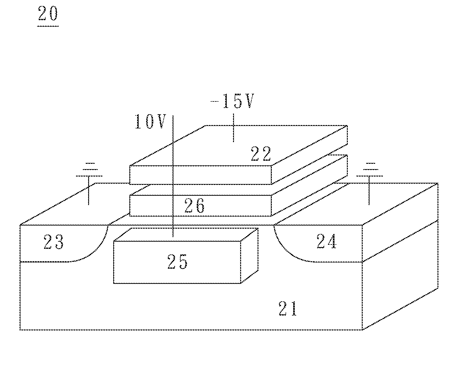
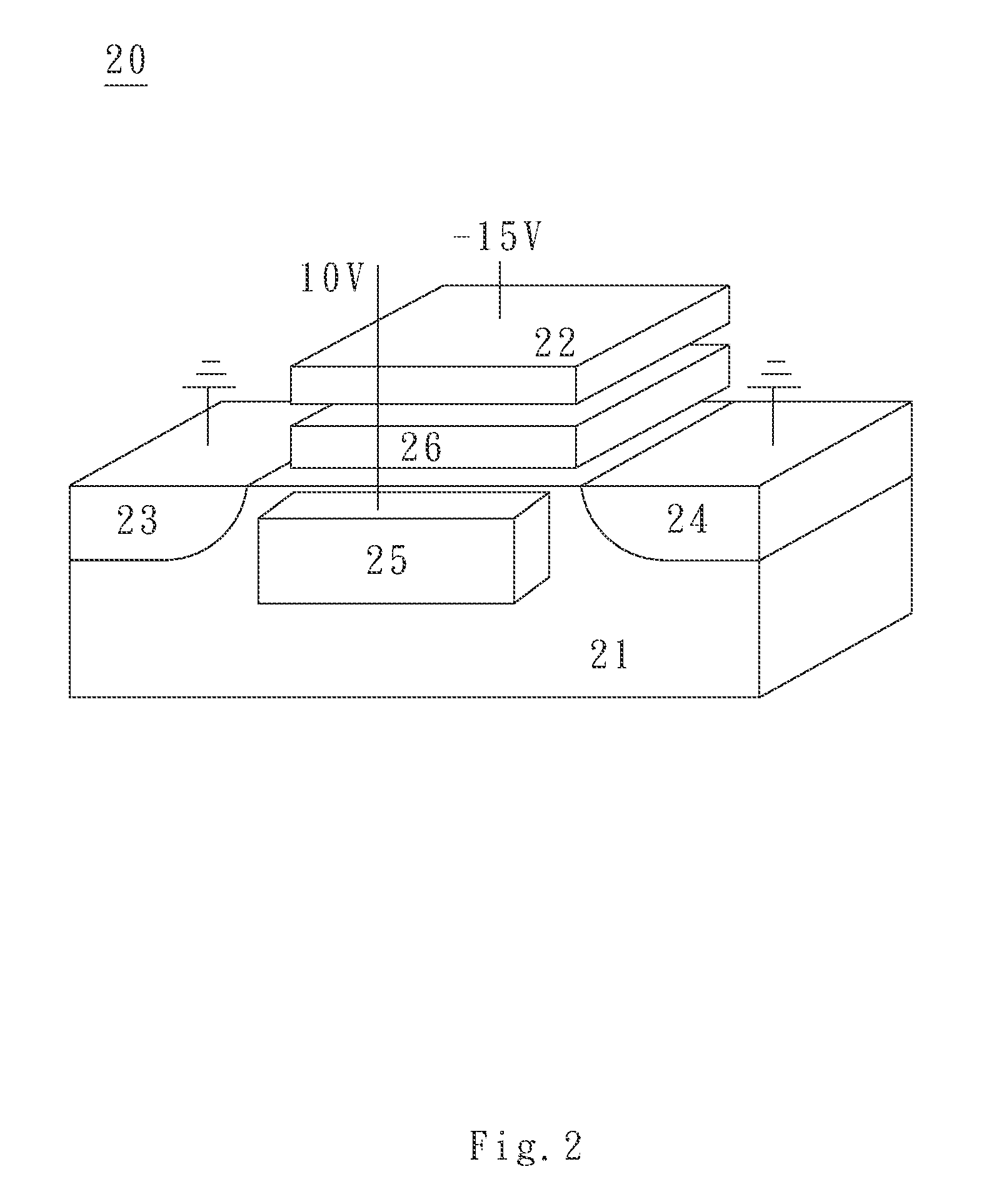
[0009]FIG. 1 is a diagram showing erasing voltages according to the first embodiment of the invention. Referring to FIG. 1, the present invention uses a nonvolatile memory (20) which is a flash type nonvolatile memory. For instance, with N-channel, the nonvolatile memory (20) includes a p-type body (21), a gate (22), a heavy doped N-type source (23), a heavy doped N-type drain (24), a heavy doped P-type body contact (25) formed on the bottom of the body (21) and a storage layer (26) formed between the gate (22) and the body (21), wherein the nonvolatile memory (20) could be a floating gate or a SONOS type memory. An erasing method for the nonvolatile memory according to the invention comprises providing a first voltage ranged between −12V to −15V, to the gate (22), the first voltage...


PUM


Abstract

The present invention relates to an erasing method for nonvolatile memory, which uses forward bias between the source / drain region and body contact to inject majority carriers into the body, and then accelerates the majority carriers by an electric field between the body and the gate to energize the majority carriers to overcome the oxide barrier and to erase the nonvolatile memory.

Description

FIELD OF THE INVENTION[0001]The present invention relates to an erasing method for a nonvolatile memory, and in particular to an erasing method for a nonvolatile memory by using a body contact.BACKGROUND OF THE INVENTION[0002]As a result of the nonvolatile memory widely used in the electrical devices in recent years, requirements of the nonvolatile memory with high performance have raised, and different types of flash type nonvolatile memory have been developed such as types of floating gate, SONOS, etc. Performances of those memories are affected by manipulation methods of those memories, and the erasing method for nonvolatile memory is very critical to such purpose.[0003]Currently, there are two main techniques about erasing method for flash type nonvolatile memory, which use Fowler-Nordheim tunneling effect and band-to-band hot hole effect. However, one of the mentioned methods, Fowler-Nordheim tunneling effect, needs great erasing voltage and erasing time. In order to decrease t...

Claims


Application Information

Patent Timeline
Patent Type & Authority Applications(United States)
IPC IPC(8): G11C16/04
CPCG11C16/14G11C16/0408
Inventor CHANG, TING-CHANGJIAN, FU-YENLI, HUNG-WEI
Owner ACER INC
Why Eureka
Try Eureka