Eeprom

a technology of eeprom and eeprom, which is applied in the direction of semiconductor devices, electrical apparatus, transistors, etc., can solve the problems of unbalance of charge supply efficiency and difference between a time required for programming, and achieve the effect of reducing the difference between the programming time and the erasing time, improving the supply efficiency of holes/electrons at the time of programming/erasing, and reducing the erasing tim

Inactive Publication Date: 2007-05-31
NEC ELECTRONICS CORP
View PDF11 Cites 12 Cited by
  • Summary
  • Abstract
  • Description
  • Claims
  • Application Information

AI Technical Summary

Benefits of technology

[0011] In the EEPROM thus constructed, for example, the fist diffusion layer is an N+ diffusion layer as an electron supply source, while the second diffusion layer is a P+ diffusion layer as a hole supply source. Both of the N+ diffusion layer and the P+ diffusion layer as the supply sources are not located away from the tunneling region but provided to contact the tunneling region. Therefore, the supply efficiencies of holes / electrons at the time of programming / erasing are improved.
[0012] Furthermore, the contact width of the N+ diffusion layer with respect to the tunneling region is substantially equal to that of the P+ diffusion layer. As a result, an unbalance of the charge supply efficiency between in the programming and in the erasing is eliminated. In other words, a difference between the programming time and the erasing time is reduced. Since an extreme increase in the programming time or the erasing time is prevented, the programming / erasing characteristics of the EEPROM are improved. In a case where the P+ diffusion layer and the N+ diffusion layer are provided separately to face each other across the first region, it is possible to easily make the above-mentioned contact widths equal to each other, which is preferable from a viewpoint of manufacturing process.
[0013] According to the nonvolatile memory cell (EEPROM) of the present invention, the unbalance of the charge supply efficiency between in the programming and in the erasing is eliminated, and thus the difference between the programming time and the erasing time is reduced. Since an extreme increase in the programming time or the erasing time is prevented, the programming / erasing characteristics of the EEPROM are improved.

Problems solved by technology

Such an unbalance of the charge supply efficiency causes a difference between a time required for the programming and a time required for the erasing.

Method used


Image

  • Eeprom
  • Eeprom
  • Eeprom

Examples


first embodiment

1. First Embodiment

[0031] 1-1. Structure and Principle

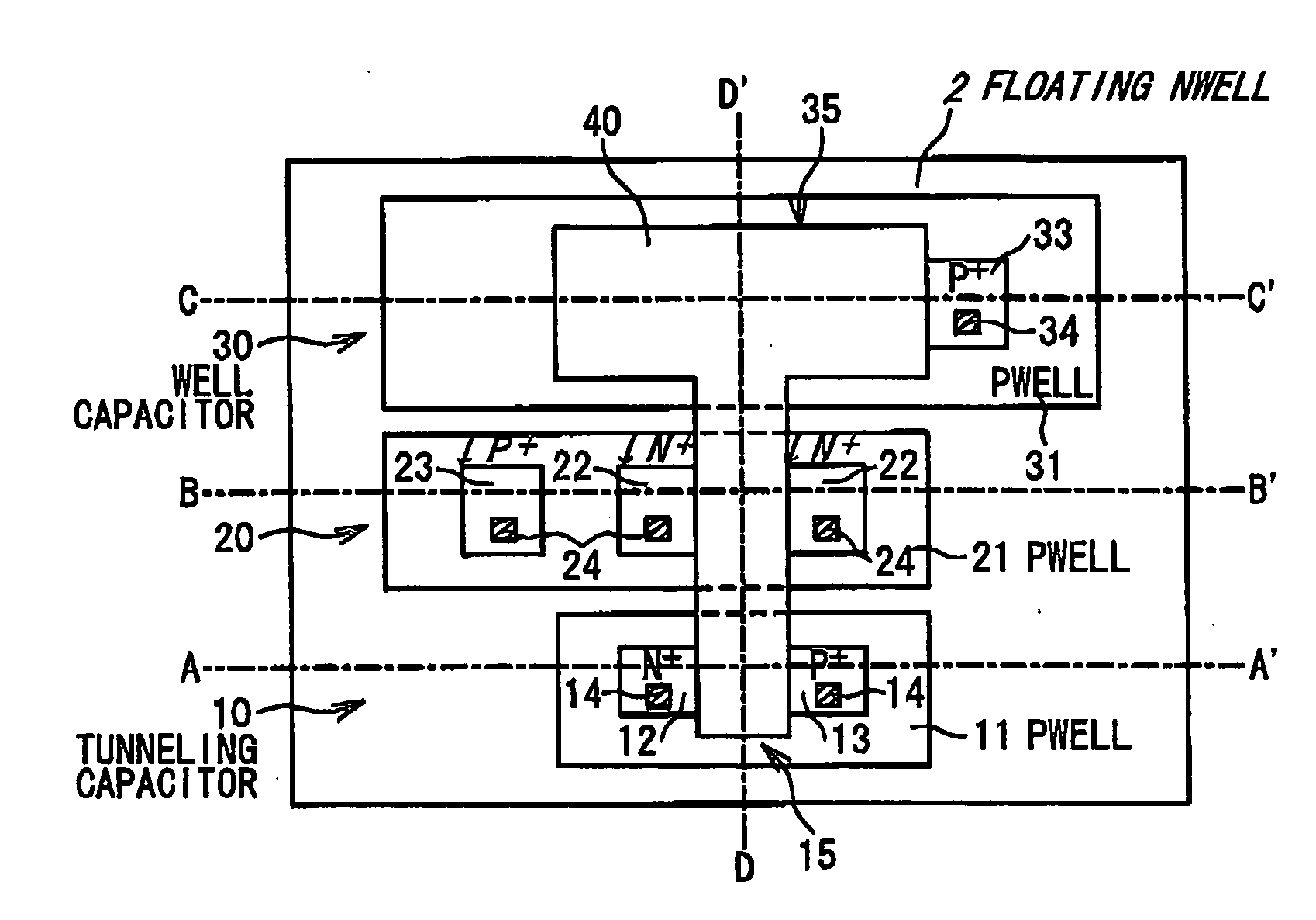
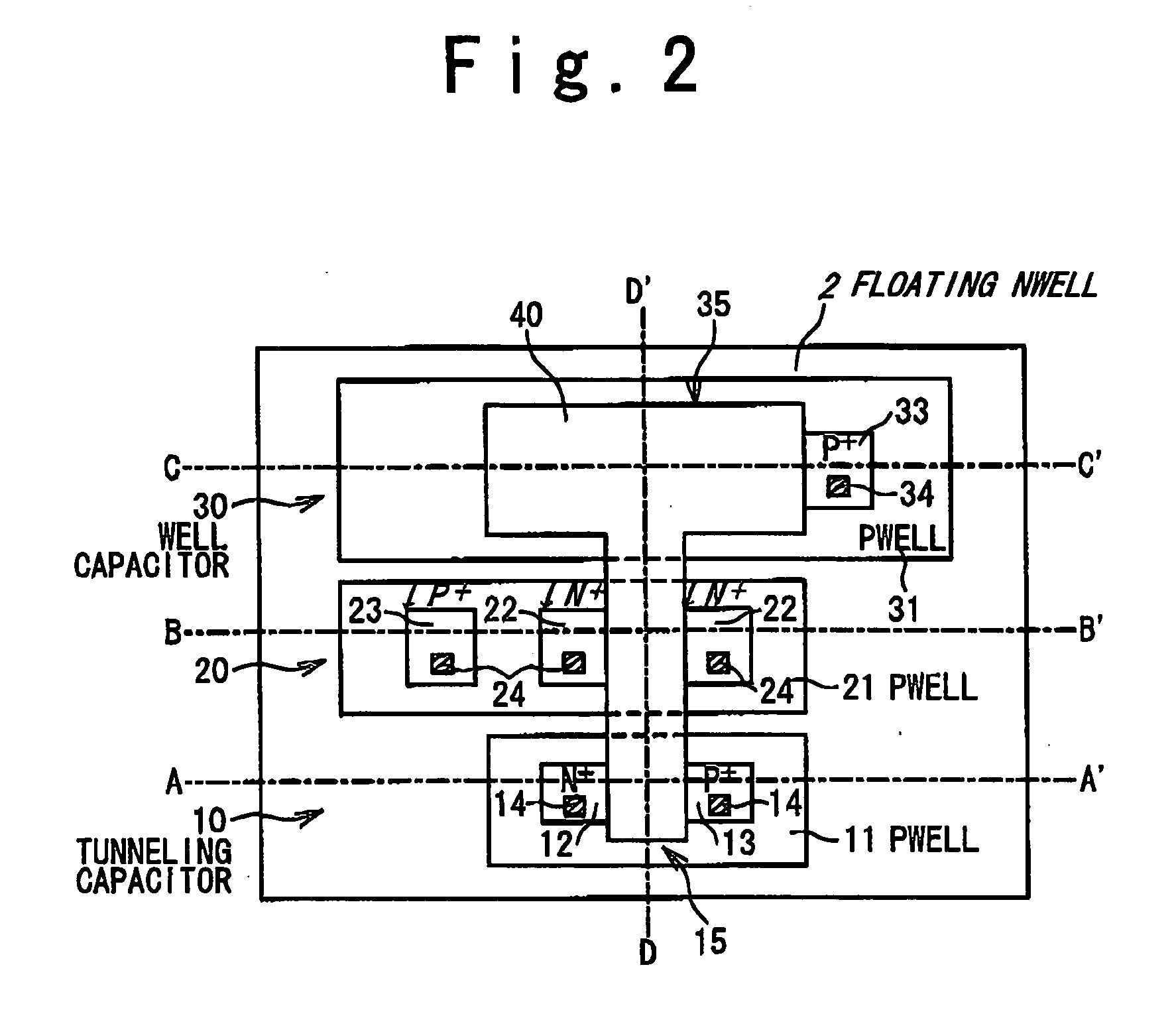
[0032]FIG. 2 is a plan view showing a structure of the nonvolatile memory cell (EEPROM) according to a first embodiment of the present invention. Cross-sectional structures along a line A-A′, a line B-B′, a line C-C′ and a line D-D′ in FIG. 2 are illustrated in FIG. 3A, FIG. 3B, FIG. 3C and FIG. 3D, respectively.

[0033] As shown in FIG. 2, the nonvolatile memory cell according to the present embodiment has a tunneling capacitor 10, a read transistor 20 and a well capacitor 30. Furthermore, a floating gate 40 is provided with respect to the tunneling capacitor 10, the read transistor 20 and the well capacitor 30.

[0034] Referring to FIG. 2, the tunneling capacitor 10 is constituted by a P-well 11 and the floating gate 40. A region in which the floating gate 40 overlaps the P-well 11 is hereinafter referred to as a “tunneling region 15”. An N+ diffusion layer 12 and a P+ diffusion layer 13 are so formed in the P-well 11 as to cont...

second embodiment

2. Second Embodiment

[0057]FIG. 8 is a plan view showing a structure of a nonvolatile memory cell (EEPROM) according to a second embodiment of the present invention. In FIG. 8, the same reference numerals are given to the same components as those described in the first embodiment, and a redundant description will be appropriately omitted. The nonvolatile memory cell according to the second embodiment has the tunneling capacitor 10, the read transistor 20 and a well capacitor 30′. The configuration of the tunneling capacitor 10 is the same as that in the first embodiment. Therefore, the same effects as those in the first embodiment can be obtained.

[0058] In the present embodiment, not only the P+ diffusion layer 33 but also an N+ diffusion layer 32 is formed in the P-well 31 of the well capacitor 30′. The N+ diffusion layer 32 and the P+ diffusion layer 33 are so formed as to contact the overlap region 35 where the floating gate 40 overlaps the P-well 31.

[0059]FIG. 9 is a view corre...

third embodiment

3. Third Embodiment

[0066]FIG. 11 is a plan view showing a structure of a nonvolatile memory cell (EEPROM) according to a third embodiment of the present invention. In FIG. 11, the same reference numerals are given to the same components as those described in the first embodiment, and a redundant description will be appropriately omitted. The nonvolatile memory cell according to the third embodiment has two elements of the tunneling capacitor 10 and the read transistor 20. As compared with the foregoing embodiments, the well capacitor 30 is omitted.

[0067] In the present embodiment, the read transistor 20 serves as the well capacitor 30 in the first embodiment. That is to say, the read transistor 20 is used not only in the read operation but also in the programming / erasing operations. In the programming / erasing operations, a first potential is applied to the N+ diffusion layer 12 and the P+ diffusion layer 13 of the tunneling capacitor 10. Furthermore, a second potential is applied t...


PUM


Abstract

An EEPROM having a nonvolatile memory cell is provided. The nonvolatile memory cell has: a first well formed in a substrate; a floating gate formed on the substrate through a gate insulating film to overlap a first region of the first well; and first and second diffusion layers formed in the first well to contact the first region. A charge supply to the floating gate is performed through the gate insulating film between the first region and the floating gate. The first diffusion layer and the second diffusion layer are of opposite conductivity types and are provided such that efficiencies of the charge supply to the floating gate from respective of the first diffusion layer and the second diffusion layer are equal to each other.

Description

BACKGROUND OF THE INVENTION [0001] 1. Field of the Invention [0002] The present invention relates to a nonvolatile memory, and particularly relates to an EEPROM (Electrically Erasable and Programmable Read Only Memory). [0003] 2. Description of the Related Art [0004] An EEPROM is known as a nonvolatile memory capable of electrically programming and erasing data. A “single poly EEPROM” is a type of the EEPROM, which does not have a stacked gate but a single-layer gate. Such a single poly EEPROM is disclosed, for example, in the following patent documents. [0005] An EEPROM described in Japanese Laid-Open Patent Application JP-H06-334190 has: an NMOS transistor formed on a P-type substrate; a PMOS transistor formed on an N-well in the P-type substrate; and a single-layer polysilicon (floating gate) formed on the P-type substrate through a gate insulating film. The single-layer polysilicon is not only a gate electrode of the NMOS transistor but also a gate electrode of the PMOS transist...

Claims


Application Information

Patent Timeline
Patent Type & Authority Applications(United States)
IPC IPC(8): H01L29/788
CPCH01L29/42324H01L29/7883H10B41/30
Inventor TANAKA, KOUJI
Owner NEC ELECTRONICS CORP
Why Eureka
Try Eureka