

Thin film transistor and display unit
a thin film transistor and display unit technology, applied in the direction of transistors, organic semiconductor devices, thermoelectric devices, etc., can solve the problems of hard restoration of the transistor characteristics, suppress leakage current, and reduce the resistance of the oxide semiconductor layer , the effect of light display
Active Publication Date: 2010-08-12
JOLED INC
View PDF16 Cites 88 Cited by
- Summary
- Abstract
- Description
- Claims
- Application Information
AI Technical Summary
Benefits of technology
[0009]It is desirable to provide a thin film transistor with which oxygen is easily supplied to an oxide semiconductor layer and favorable transistor characteristics are able to be restored, and a display unit including the thin film transistor.
[0021]The first to the third display units of the embodiment of the invention respectively include the first to the third thin film transistors of the embodiment of the invention. Thus, low resistance of the oxide semiconductor layer of the thin film transistor is inhibited and thus the leakage current is able to be suppressed, and light display with high luminance is enabled.
Problems solved by technology
However, there has been a disadvantage that the transistor characteristics are hardy restored according to the shape and the size of a TFT.
Method used
View moreImage
Smart ImageViewing Examples

Examples
first embodiment (
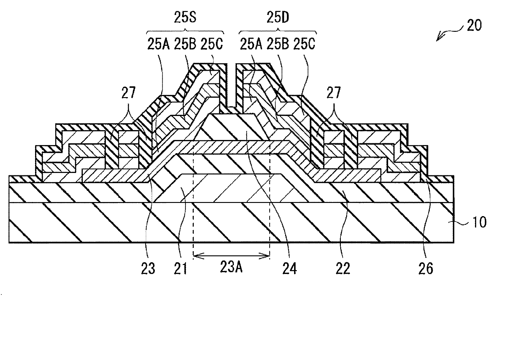
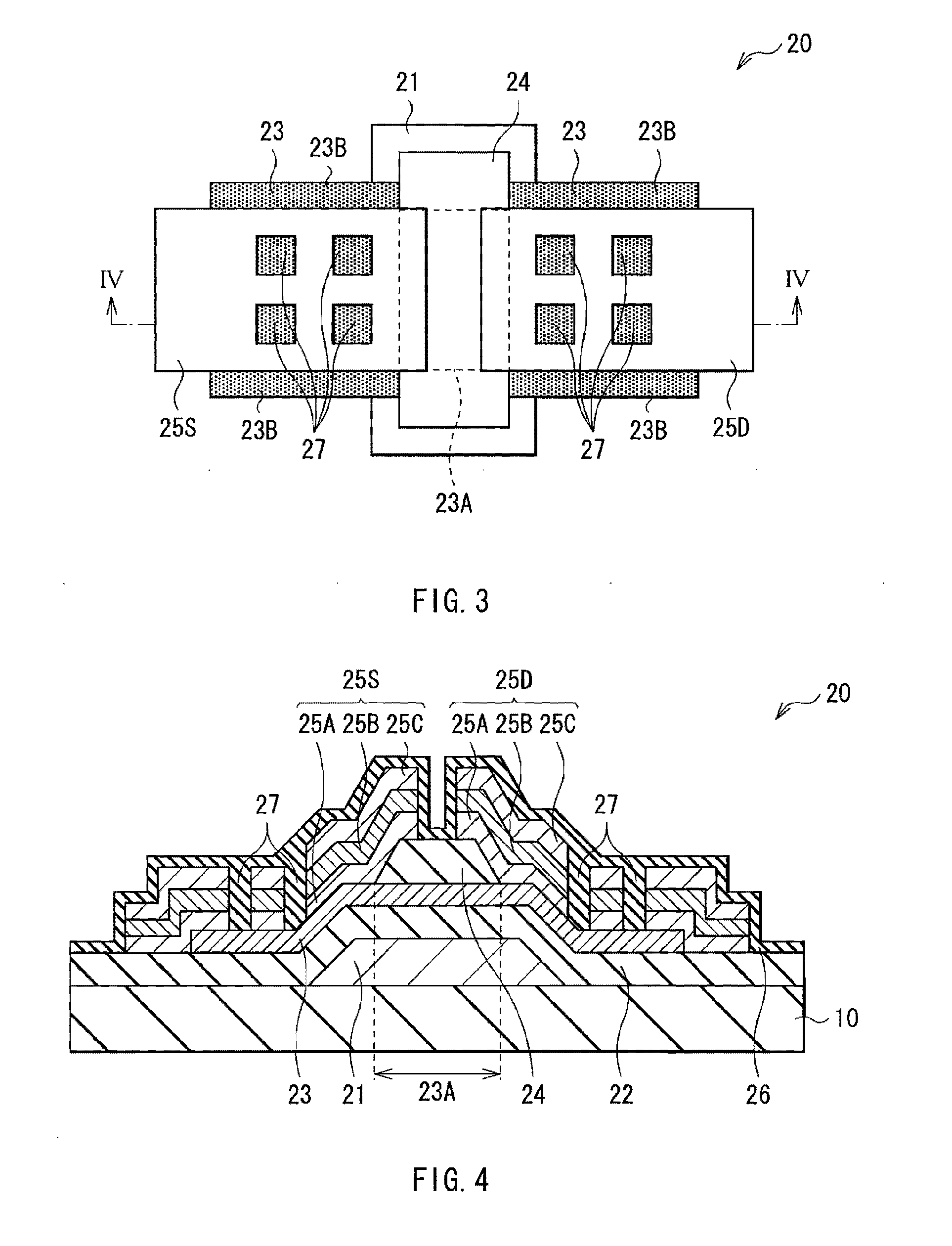
1. First embodiment (example that an aperture is provided in a source electrode and a drain electrode);
second embodiment (
2. Second embodiment (example that the source electrode and the drain electrode are isolated by a groove); and
third embodiment (
3. Third embodiment (example that a protrusion region is provided outside the source electrode and the drain electrode).
Login to View More PUM
 Abstract
A thin film transistor with which oxygen is easily supplied to an oxide semiconductor layer and favorable transistor characteristics are able to be restored and a display unit including the same are provided. The thin film transistor includes sequentially over a substrate a gate electrode, a gate insulting film, an oxide semiconductor layer including a channel region, and a channel protective layer covering the channel region A source electrode and a drain electrode are formed on the oxide semiconductor layer located on both sides of the channel protective layer, and at least one of the source electrode and the drain electrode has an aperture to expose the oxide semiconductor layer.
Description
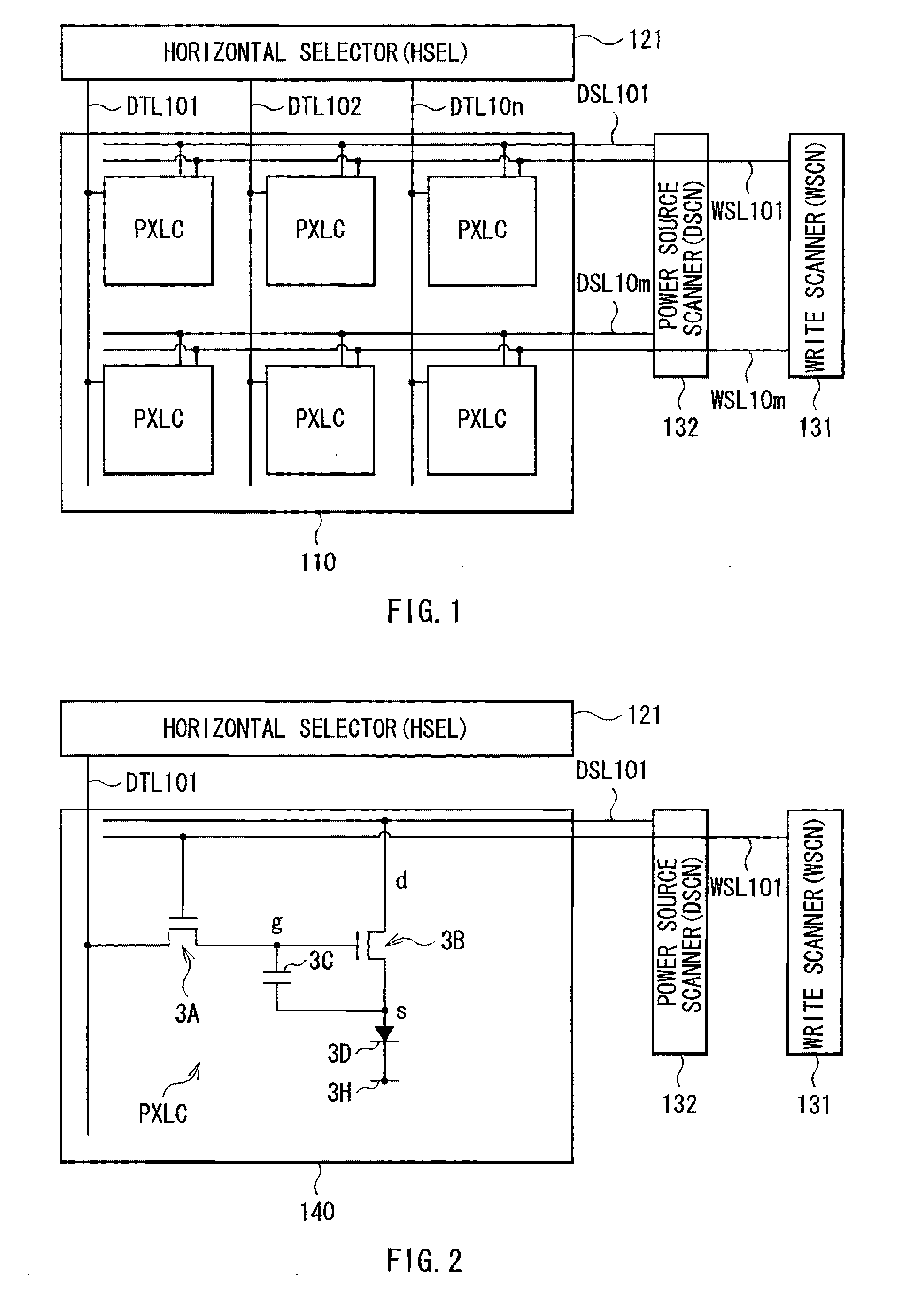
BACKGROUND OF THE INVENTION[0001]1. Field of the Invention[0002]The present invention relates to a thin film transistor (TFT) having an oxide semiconductor layer as a channel and a display unit including the same.[0003]2. Description of the Related Art[0004]An oxide semiconductor composed of, for example, a zinc oxide, an indium gallium zinc oxide (IGZO) or the like shows superior characteristics as an active layer of a semiconductor device. In recent years, development has been promoted in an effort to apply the oxide semiconductor to a TFT, a light emitting device, a transparent conducting film or the like.[0005]For example, in the TFT including the oxide semiconductor, electron mobility is high and its electric characteristics are superior compared to the existing TFT including amorphous silicon (a-Si: H) used for a liquid crystal display unit as a channel. Further, the TFT including the oxide semiconductor has an advantage that high mobility is able to be expected even at low te...
Claims
Login to View More Application Information
Patent Timeline
 Patent Type & AuthorityApplications(United States)
IPC IPC(8): H01L51/52H01L29/786
CPCH01L27/1225H01L27/3262H01L29/41733H01L29/66969H01L29/78606H01L29/7869H01L2251/5315H01L29/458H10K59/1213H10K2102/3026H01L29/66742H01L29/78696
InventorARAI, TOSHIAKIMOROSAWA, NARIHIROTOKUNAGA, KAZUHIKOSAGAWA, HIROSHIMIURA, KIWAMU
OwnerJOLED INC