Semiconductor apparatus, manufacturing method of semiconductor apparatus, and joint material
Active Publication Date: 2009-04-16
RENESAS ELECTRONICS CORP
View PDF19 Cites 81 Cited by
Summary
Abstract
Description
Claims
Application Information
AI Technical Summary
This helps you quickly interpret patents by identifying the three key elements:
Problems solved by technology
Method used
Benefits of technology
Benefits of technology
[0007]As the characteristics required in the actual die bonding material and process of the semiconductor apparatus, the mass productivity equivalent to that of the conventional high-Pb-content solder is required in the production process. More specifically, characteristics such as (a) supply of the joint material is easy, (b) process temperature is 350° C. or lower in the light of heat resistant properties of the components, (c) joint can be made by the pressureless process in the light of the mass productivity, (d) large void failure does not occur in a joint layer in the light of the joint quality and others are required. Further, in order to ensure the electric properties and the long-term reliability required for the semiconductor apparatus in the completed product, characteristics such as (e) thermal stress relieving function for preventing the chip crack, (f) sufficient thermal fatigue life, (g) high conductivity and high heat dissipation more than those of high-Pb-content solder and others are required for the joint portion. The alternative material of the high-Pb-content solder has to be the lead-free joint material that can satisfy the characteristics (a) to (d) at the same time, and the joint portion of the semiconductor apparatus assembled with the joint material has to satisfy all the characteristics (e) to (g). In addition, it is needless to say that the completed product is preferably manufactured at low cost.
[0027]Further, since the joint material is in paste form containing metal powders with the maximum particle diameter of 15 μm to 200 μm whose outermost surfaces are coated with precious metal, metallo-organic silver compound dissociated at the temperature of 350° C. or lower and solvent, the semiconductor part and the conductive member can be jointed at the low temperature of 350° C. or lower in the atmosphere without applying pressure, and it is possible to provide the manufacturing method of a semiconductor apparatus excellent in mass productivity and joint quality.
Problems solved by technology
Although the Zn series solder and the Sn—Sb series high-temperature solder that are the candidates of an alternative material of a Pb-free substance have sufficient heat resistant properties better than the high-Pb-content solder, because the solder material itself is hard, they have a problem that the chip crack frequently occurs in a cooling process after the die bonding.
Further, although the high-conductive silver paste has sufficient heat and electric conductivities and the reflow resistance of 260° C., it has the problem that the peeling occurs in a short time depending on the humidity environment and temperature cycle environment and required reliability cannot be obtained.
However, since application of pressure is necessary in this process, batch processing cannot be performed, and the mass productivity is inferior due to the long bonding time.
Method used
Image
Click on the blue label to locate the original text in one second.
Reading with bidirectional positioning of images and text.
Examples
first embodiment
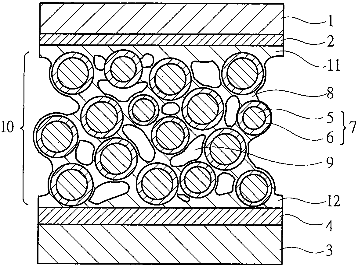
[0049]FIG. 1 shows an example of a cross-sectional structure of a die bonding portion in a semiconductor apparatus according to the first embodiment.
[0050]A chip (semiconductor part) 1 is formed of an Si (silicon) substrate about 4 mm and 5 mm on a side and about 0.26 mm thick, and semiconductor elements (power transistor elements such as power MOSFETs) are formed in a direction vertical to a surface of the Si substrate.
[0051]A rear-surface electrode 2 is configured to have a multi-layered structure obtained by stacking an Al (aluminum) film, a Ti (titanium) film, an Ni (nickel) film and an Au (gold) film in this order from the side of the chip 1, and the Au film is the outermost film. Note that a V (vanadium) film may be used instead of the Al film.
[0052]A die pad (conductive member, second conductive member) 3 is formed of a lead frame made of Cu (copper) plated with Ni. Further, a plating film 4 made of Ag (silver) or Ni with a thickness of about 5 μm is formed on a surface of th...
second embodiment
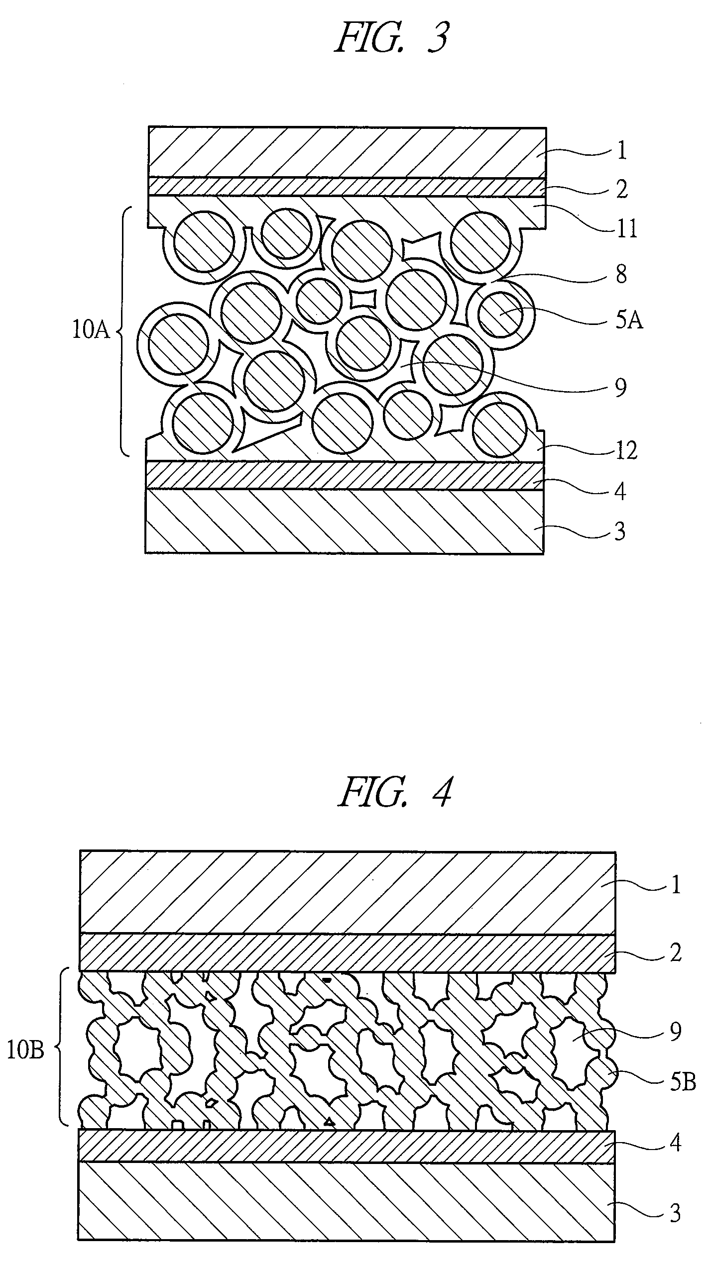
[0059]FIG. 3 shows an example of a cross-sectional structure of a die bonding portion in a semiconductor apparatus according to the second embodiment.
[0060]In FIG. 3, the chip 1, the rear-surface electrode 2, the die pad 3 and the plating film 4 are the same as those described in the first embodiment with reference to FIG. 1.
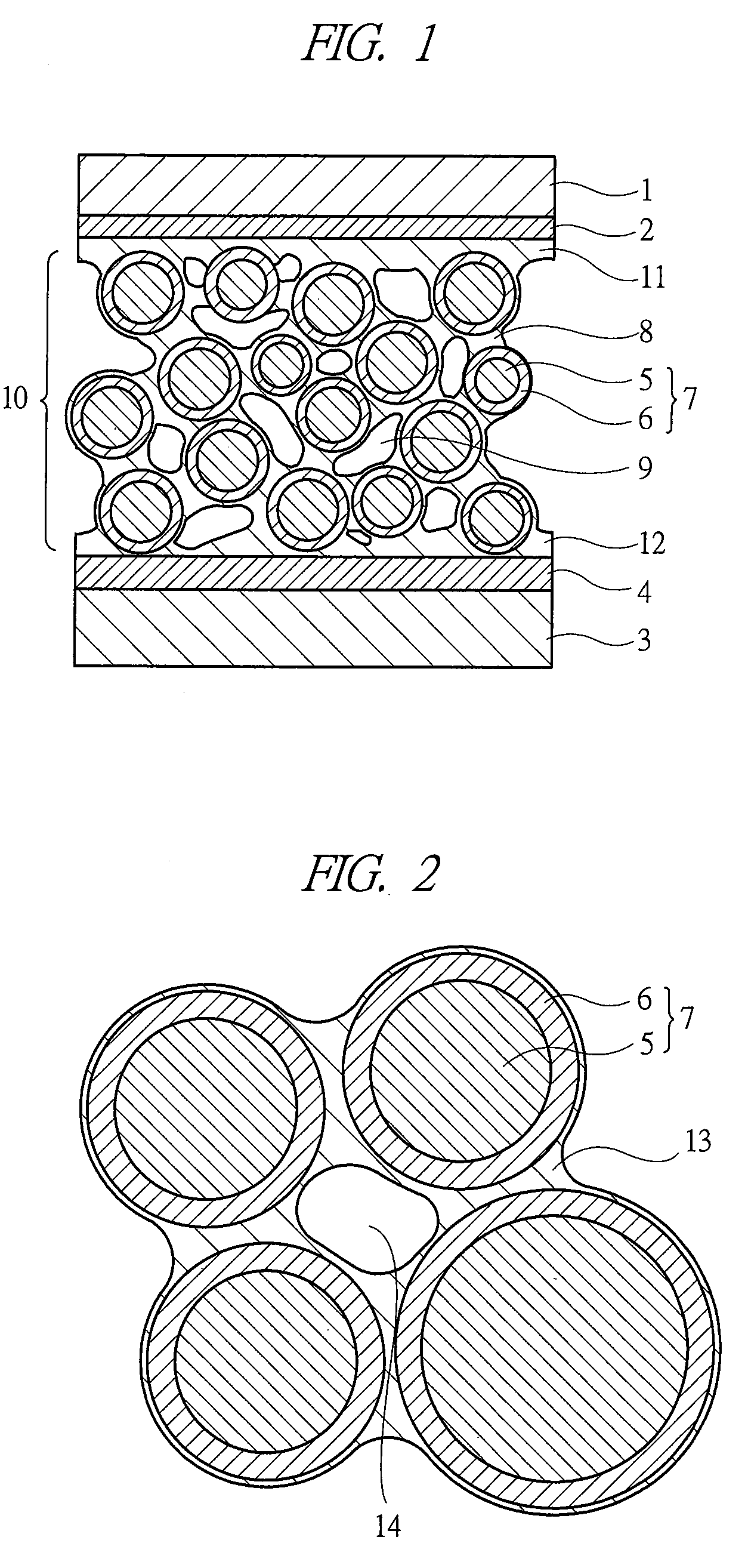
[0061]The chip 1 and the die pad 3 are electrically connected by single metal powders 5A and the adhesivelayers 8, 11 and 12, and the joint layer (bonding layer) 10A between the chip 1 and the die pad 3 is formed of the single metal powders 5A, the adhesivelayers 8, 11 and 12, and the holes 9. The single metal powders 5A are made of Cu single metal powders with a diameter of about 10 μm to 100 μm fabricated by the atomize method, and the surface thereof is coated with precipitated and fused Ag. In the assembly process of a semiconductor apparatus, when the heat treatment is performed in an atmosphere, the surface of Cu is oxidized and an oxide film is formed, ...
third embodiment
[0063]FIG. 4 shows an example of a cross-sectional structure of a die bonding portion in a semiconductor apparatus according to the third embodiment.
[0064]In FIG. 4, the chip 1, the rear-surface electrode 2, the die pad 3 and the plating film 4 are the same as those described in the first embodiment with reference to FIG. 1.
[0065]In the third embodiment, silver metal powders 5B are used for the joint material (joint layer 10B). Therefore, the internal structure of the joint layer (bonding layer) 10B appears similar to that of an adhesive layer made of Ag with many gaps.
[0066]According to the third embodiment, the chip 1 and the die pad 3 are bonded by only mechanically flexible Ag, and the inside of the joint layer 10B is formed to have a porous structure (holes 9 are formed) and is easily deformed. Therefore, the thermal stress load applied to the chip 1 can be reduced, and the thickness of the joint layer 10B can be determined by the thickness at the time when the chip 1 is mounte...
PUM
Property
Measurement
Unit
Temperature
aaaaa
aaaaa
Temperature
aaaaa
aaaaa
Temperature
aaaaa
aaaaa
Abstract
A die bonding portion is metallically bonded by well-conductive Cu metal powders with a maximum particle diameter of about 15 μm to 200 μm and adhesivelayers of Ag, and minute holes are evenly dispersed in a joint layer. With this structure, the reflow resistance of about 260° C. and reliability under thermal cycle test can be ensured without using lead.
Description
CROSS-REFERENCE TO RELATED APPLICATION[0001]The present application claims priority from Japanese Patent Application No. JP 2007-264412 filed on Oct. 10, 2007, the content of which is hereby incorporated by reference into this application.TECHNICAL FIELD OF THE INVENTION[0002]The present invention relates to a semiconductor apparatus, a manufacturing technology of a semiconductor apparatus and a joint material. More particularly, it relates to a lead-free semiconductor apparatus provided with an electrode joint structure having a reflow resistance of about 260° C. and high reliability under thermal cycle test, a low-cost joint material capable of and low-temperature process for obtaining the joint structure, and a manufacturing technology of the semiconductor apparatus excellent in mass productivity.BACKGROUND OF THE INVENTION[0003]A power semiconductor apparatus typified by a power transistorpackage or the like has a packaging structure in which a rear-surface electrode of a semic...
Claims
Application Information
Patent Timeline
Application Date:The date an application was filed.
Publication Date:The date a patent or application was officially published.
First Publication Date:The earliest publication date of a patent with the same application number.
Issue Date:Publication date of the patent grant document.
PCT Entry Date:The Entry date of PCT National Phase.
Estimated Expiry Date:The statutory expiry date of a patent right according to the Patent Law, and it is the longest term of protection that the patent right can achieve without the termination of the patent right due to other reasons(Term extension factor has been taken into account ).
Invalid Date:Actual expiry date is based on effective date or publication date of legal transaction data of invalid patent.

