

Semiconductor device
- Summary
- Abstract
- Description
- Claims
- Application Information
AI Technical Summary
Benefits of technology
Problems solved by technology
Method used
Image

Examples
Embodiment Construction
[0032]Hereafter, various embodiments of the present invention will be described in detail with reference to the accompanying drawings.
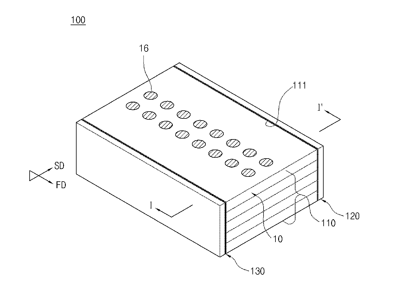
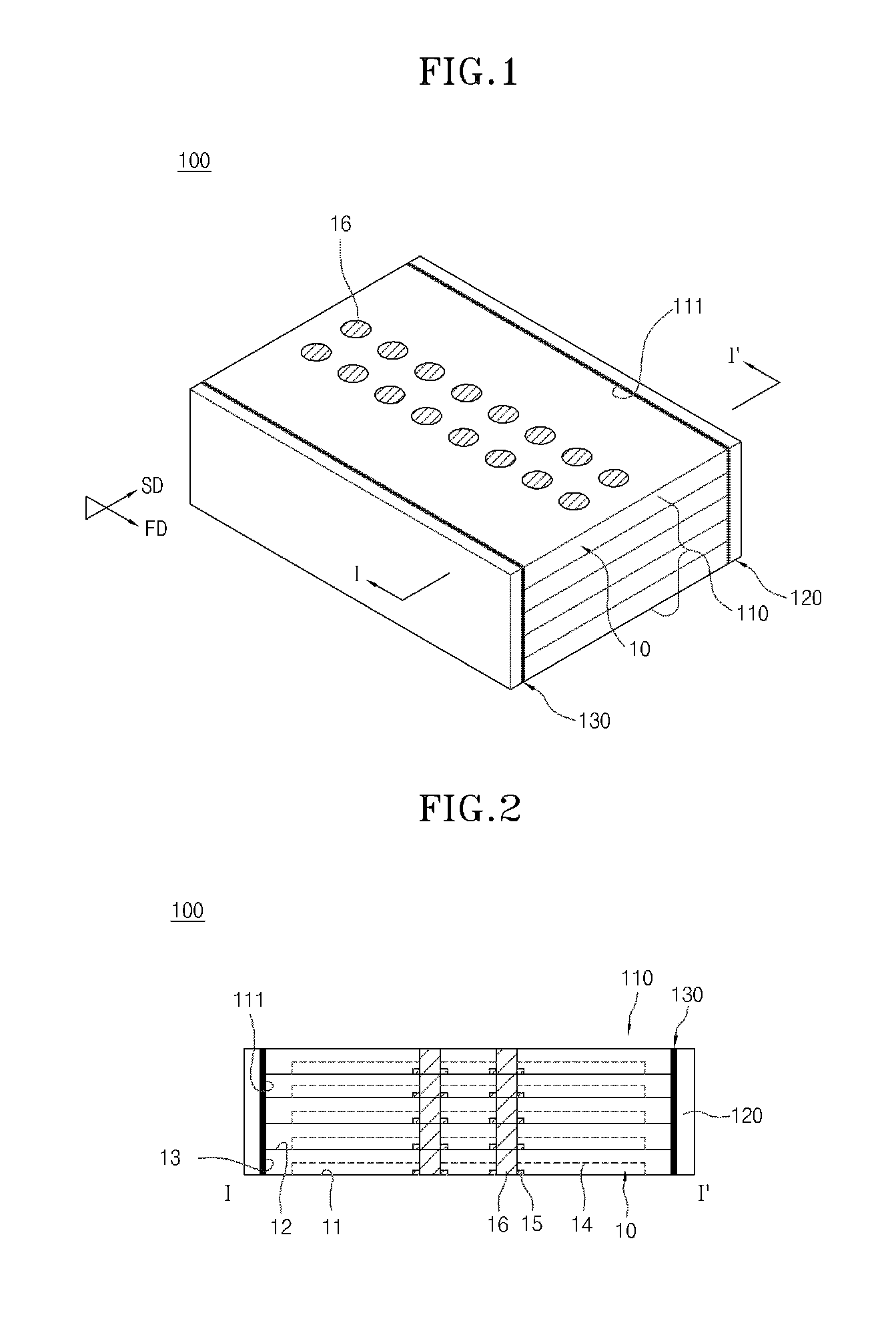
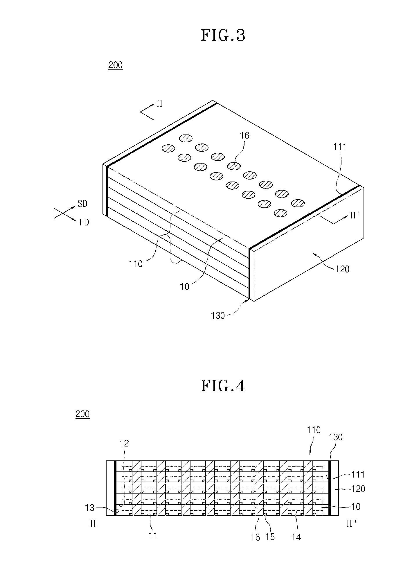
[0033]FIG. 1 is a perspective view illustrating a semiconductor device in accordance with the first embodiments andFIG. 2 is a cross-sectional view taken along a line I-I′ of FIG. 1.
[0034]Referring to FIGS. 1 and 2, a semiconductor device 100 in accordance with the first embodiments may include a chip stack structure 110 and support frames 120. The semiconductor device 100 may further include an adhesive member 130.
[0035]In the present embodiment, the chip stack structure 110 includes a plurality of first semiconductor chips 10.
[0036]Each of the first semiconductor chips 10 may substantially have a rectangular hexahedral shape. The rectangular hexahedral shaped first semiconductor chip 10 may have a first surface 11, a second surface 12 and four side surfaces 13. The first surface 11 may be opposite to the second surface 12 and the four side surfaces ...
PUM
 Abstract
Description
Claims
Application Information