Optically coupled semiconductor device and electronic device
Inactive Publication Date: 2007-11-29
SHARP KK
View PDF4 Cites 0 Cited by
Summary
Abstract
Description
Claims
Application Information
AI Technical Summary
This helps you quickly interpret patents by identifying the three key elements:
Problems solved by technology
Method used
Benefits of technology
Benefits of technology
[0020]With this configuration, both the upper and lower faces of the resin sealing portion are held by the extended portions of the U-shaped radiator, and thus the area in which heat is dissipated from the resin sealing portion is increased. Accordingly, the heat dissipation properties are improved, and thus an effective current at a high temperature can be increased, so that an optically coupled semiconductor device with a high reliability is obtained. Furthermore, the U-shaped radiator is formed into a simple shape that does not fall off the resin sealing portion, and thus production failures can be reduced in the production processes or while it is mounted. Thus, a low cost optically coupled semiconductor device with a good productivity is obtained.
[0046]With this configuration, heat is conducted directly from the U-shaped radiator to the mounting board without passing through space. Thus, heat dissipation to the mounting board can be ensured, so that the heat dissipation properties can be further improved.
Problems solved by technology
When the optically coupled semiconductor device 101 is left without taking any measure, the properties are deteriorated, and the reliability is lowered.
Thus, there is a problem in that the radiator 121 lacks reliability, for example, due to a possibility of falling off the resin sealing portion 116.
However, these radiators have complicated configurations, and cannot be easily attached.
Even when the radiators can be easily attached, there is a problem in the attachment strength.
However, in the conventional optically coupled semiconductor device, a radiator or heat dissipating terminal is separately and independently formed, and thus high heat dissipation cannot be realized.
Furthermore, in a configuration where a lead frame is extended, or a radiator is exposed on a side face of the package, it is necessary to use a large number of special materials and equipment in production processes, and thus the cost increases.
Method used
Image
Click on the blue label to locate the original text in one second.
Reading with bidirectional positioning of images and text.
Examples
embodiment 1
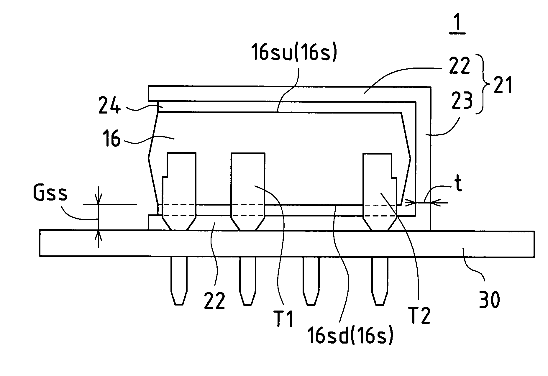
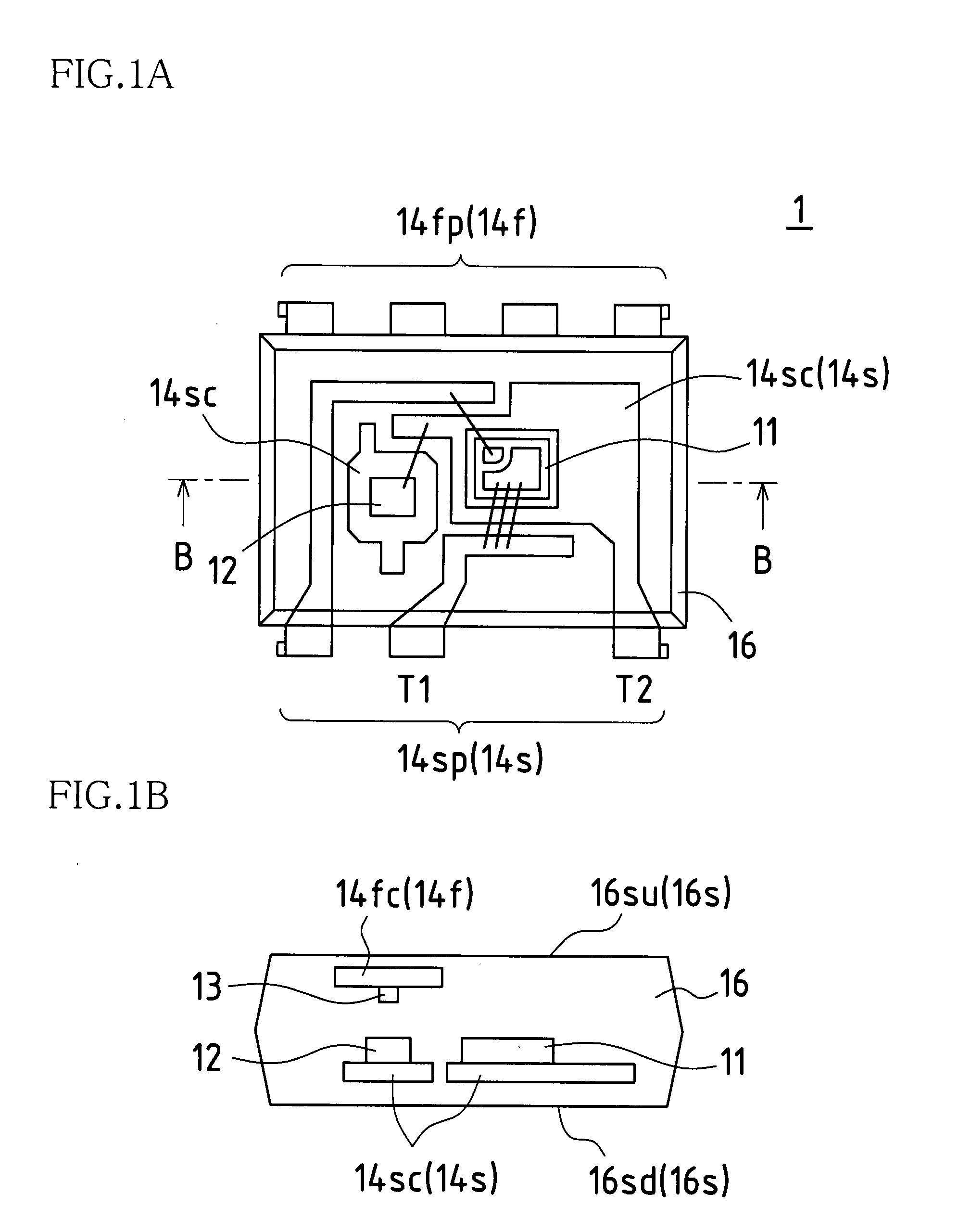
[0080]An optically coupled semiconductor device according to Embodiment 1 of the present invention is described with reference to FIGS. 1A, 1B, 2A, and 2B.
[0081]FIG. 1A is a see-through plan view illustrating the outline of an optically coupled semiconductor device according to Embodiment 1 of the present invention before a U-shaped radiator is engaged therewith, showing a plane with a power control semiconductor element from the side of a light-emitting element chip. FIG. 1B is a see-through side view showing the main portions on a cross section of FIG. 1A, viewed in the direction indicated by the arrow B. In FIG. 1B, hatching has been omitted.
[0082]An optically coupled semiconductor device 1 has a primary-side lead frame 14f and a secondary-side lead frame 14s that are opposed to each other. On the inner side on the secondary-side lead frame 14s, a plurality of chip mounting portions 14sc are formed that are substantially on the same plane. A power control semiconductor element ch...
embodiment 2
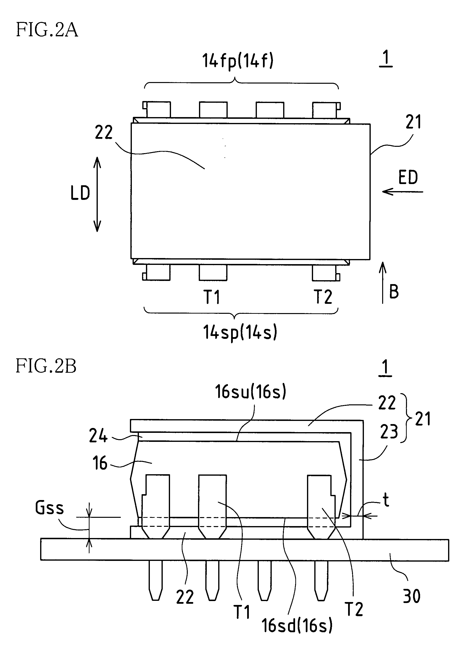
[0098]An optically coupled semiconductor device according to Embodiment 2 of the present invention is described with reference to FIGS. 3A, 3B, 4A, and 4B.
[0099]FIG. 3A is a plan view showing an optically coupled semiconductor device according to Embodiment 2 of the present invention. FIG. 3B is a side view of FIG. 3A, viewed in the direction indicated by the arrow B. In FIG. 3B, the optically coupled semiconductor device is mounted on the mounting board 30 of an electronic device (not shown).
[0100]In this embodiment, the shape of the U-shaped radiator 21 in Embodiment 1 has been modified. The other configurations are the same as those in Embodiment 1, and thus a description thereof has been omitted as appropriate.
[0101]In a case where the inner faces of the extended portions 22 are flat as in Embodiment 1, the U-shaped radiator 21 may be displaced upward or downward with respect to the resin sealing portion 16 due to spacing (clearance) between the U-shaped radiator 21 and the seal...
embodiment 3
[0109]An optically coupled semiconductor device according to Embodiment 3 of the present invention is described with reference to FIGS. 5, 6A, and 6B.
[0110]FIG. 5 is a side view showing an unengaged U-shaped radiator for holding a resin sealing portion of an optically coupled semiconductor device according to Embodiment 3 of the present invention. In FIG. 5, the optically coupled semiconductor device 1 is not shown, but has the same configuration as those in the foregoing embodiments, and thus this embodiment is described referring to the reference numerals used in the embodiments as appropriate.
[0111]The U-shaped radiator 21 of the optically coupled semiconductor device 1 according to this embodiment has spring properties such that an opposing distance Lg between the extended portions 22 is long on the side of the linking portion 23 and is short on the side of the ends of the extended portions 22 in a state where the resin sealing portion 16 is not inserted. Accordingly, when the o...
PUM
Abstract
In an embodiment of an optically coupled semiconductor device of the present invention, the optically coupled semiconductor device is provided with a resin sealing portion and lead drawing portions. The resin sealing portion integrally seals a power controlsemiconductor element chip, an firing light-receiving element chip for firing the power control semiconductor element chip, and a light-emitting element chip optically coupled with the firing light-receiving element, for converting an electric signal into an optical signal. The lead drawing portions are connected to the power control semiconductor element chip, the firing light-receiving element, and the light-emitting element chip, and are drawn out of the resin sealing portion. The optically coupled semiconductor device is further provided with a U-shaped radiator having extended portions that extend in an extending direction intersecting a drawing direction of the lead drawing portions and that are operable to hold the resin sealing portion therebetween.
Description
[0001]This application claims priority under 35 U.S.C. § 119(a) on Patent Application No. 2006-148444 filed in Japan on May 29, 2006, the entire contents of which are hereby incorporated by reference.BACKGROUND OF THE INVENTION[0002]1. Field of the Invention[0003]The present invention relates to an optically coupled semiconductor device applied to a solid state relay and the like, and an electronic device in which the optically coupled semiconductor device is installed.[0004]2. Description of the Related Art[0005]An example of a conventional optically coupled semiconductor device is described with reference to FIG. 15. FIG. 15 is a side view showing a conventional optically coupled semiconductor device.[0006]A conventional optically coupled semiconductor device 101 is configured, for example, as a solid state relay. In the solid state relay, a power control semiconductor element chip, a light-emitting element, and a firing light-receiving element are integrally sealed with a resin s...
Claims
Application Information
Patent Timeline
Application Date:The date an application was filed.
Publication Date:The date a patent or application was officially published.
First Publication Date:The earliest publication date of a patent with the same application number.
Issue Date:Publication date of the patent grant document.
PCT Entry Date:The Entry date of PCT National Phase.
Estimated Expiry Date:The statutory expiry date of a patent right according to the Patent Law, and it is the longest term of protection that the patent right can achieve without the termination of the patent right due to other reasons(Term extension factor has been taken into account ).
Invalid Date:Actual expiry date is based on effective date or publication date of legal transaction data of invalid patent.

